SNVS345G June 2006 – December 2014 LP5951
PRODUCTION DATA.
- 1 Features
- 2 Applications
- 3 Description
- 4 Revision History
- 5 Pin Configuration and Functions
- 6 Specifications
- 7 Detailed Description
- 8 Application and Implementation
- 9 Power Supply Recommendations
- 10Layout
- 11Device and Documentation Support
- 12Mechanical, Packaging, and Orderable Information
Package Options
Mechanical Data (Package|Pins)
Thermal pad, mechanical data (Package|Pins)
Orderable Information
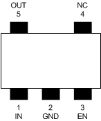
5 Pin Configuration and Functions
SOT-23 (DBV)
5 Pins
Top View
SC70 (DCK)
5 Pins
Top View
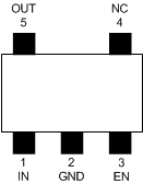
Pin Functions
| PIN | TYPE | DESCRIPTION | |
|---|---|---|---|
| NUMBER | NAME | ||
| 1 | IN | I | Input voltage 1.8 V to 5.5 V |
| 2 | GND | — | Ground |
| 3 | EN | I | Enable pin logic input: Low = shutdown, High = normal operation. This pin should not be left floating. |
| 4 | NC | — | No internal connection |
| 5 | OUT | O | Regulated output voltage |