SNVS345G June   2006  – December 2014 LP5951

PRODUCTION DATA.  

  1. Features
  2. Applications
  3. Description
  4. Revision History
  5. Pin Configuration and Functions
  6. Specifications
    1. 6.1 Absolute Maximum Ratings
    2. 6.2 ESD Ratings
    3. 6.3 Recommended Operating Conditions
    4. 6.4 Thermal Information
    5. 6.5 Electrical Characteristics
    6. 6.6 Enable Control Characteristics
    7. 6.7 Transient Characteristics
    8. 6.8 Output Capacitor, Recommended Specification
    9. 6.9 Typical Characteristics
  7. Detailed Description
    1. 7.1 Overview
    2. 7.2 Functional Block Diagram
    3. 7.3 Feature Description
      1. 7.3.1 No-Load Stability
      2. 7.3.2 Enable Operation
      3. 7.3.3 Fast Turn Off And On
      4. 7.3.4 Short-Circuit Protection
      5. 7.3.5 Thermal-Overload Protection
      6. 7.3.6 Reverse Current Path
    4. 7.4 Device Functional Modes
      1. 7.4.1 Enable (EN)
      2. 7.4.2 Minimum Operating Input Voltage (VIN)
  8. Application and Implementation
    1. 8.1 Application Information
    2. 8.2 Typical Application
      1. 8.2.1 Design Requirements
      2. 8.2.2 Detailed Design Procedure
        1. 8.2.2.1 Power Dissipation And Device Operation
        2. 8.2.2.2 External Capacitors
        3. 8.2.2.3 Input Capacitor
        4. 8.2.2.4 Output Capacitor
        5. 8.2.2.5 Capacitor Characteristics
      3. 8.2.3 Application Curves
  9. Power Supply Recommendations
    1. 9.1 Output Current Derating
  10. 10Layout
    1. 10.1 Layout Guidelines
    2. 10.2 Layout Example
  11. 11Device and Documentation Support
    1. 11.1 Device Support
      1. 11.1.1 Third-Party Products Disclaimer
    2. 11.2 Documentation Support
      1. 11.2.1 Related Documentation
    3. 11.3 Trademarks
    4. 11.4 Electrostatic Discharge Caution
    5. 11.5 Glossary
  12. 12Mechanical, Packaging, and Orderable Information

Package Options

Mechanical Data (Package|Pins)
Thermal pad, mechanical data (Package|Pins)
Orderable Information

9 Power Supply Recommendations

This device is designed to operate from an input supply voltage range of 1.8 V to 5.5 V. The input supply should be well regulated and free of spurious noise. To ensure that the LP5951 output voltage is well regulated, the input supply should be at least VOUT + 0.5 V, or 1.8 V, whichever is higher. A minimum capacitor value of 1-μF is required to be within 1 cm of the IN pin.

9.1 Output Current Derating

20136204.gif
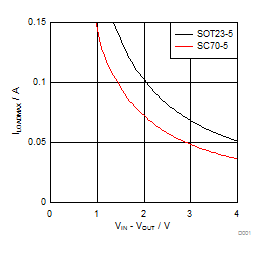
Figure 14. Maximum Load Current vs VIN – VOUT,
TA = 85°C, VOUT = 1.5 V