SNVS345G June 2006 – December 2014 LP5951
PRODUCTION DATA.
- 1 Features
- 2 Applications
- 3 Description
- 4 Revision History
- 5 Pin Configuration and Functions
- 6 Specifications
- 7 Detailed Description
- 8 Application and Implementation
- 9 Power Supply Recommendations
- 10Layout
- 11Device and Documentation Support
- 12Mechanical, Packaging, and Orderable Information
Package Options
Mechanical Data (Package|Pins)
Thermal pad, mechanical data (Package|Pins)
Orderable Information
8 Application and Implementation
NOTE
Information in the following applications sections is not part of the TI component specification, and TI does not warrant its accuracy or completeness. TI’s customers are responsible for determining suitability of components for their purposes. Customers should validate and test their design implementation to confirm system functionality.
8.1 Application Information
The LP5951 is a linear voltage regulator for digital applications designed to be stable with space-saving ceramic capacitors as small as 1 µF. Performance is specified for a -40°C to 125°C temperature range for bot the SOT-23 and SC70 packages.
8.2 Typical Application
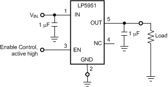 Figure 10. LP5951 Typical Application
8.2.1 Design Requirements
Table 1. Design Parameters
| DESIGN PARAMETER | DESIGN REQUIREMENT |
|---|---|
| Input voltage range | 1.8 V to 5.5 V |
| Output voltage | 1.3 V |
| Output current | 150 mA |
| Output capacitor range | 1 µF |
| Input/output capacitor ESR range | 3 mΩ to 300 mΩ |
8.2.2 Detailed Design Procedure
8.2.2.1 Power Dissipation And Device Operation
The permissible power dissipation for any package is a measure of the capability of the device to pass heat from the power source, the junctions of the IC, to the ultimate heat sink, the ambient environment. Thus, the power dissipation is dependent on the ambient temperature and the thermal resistance across the various interfaces between the die and ambient air.
In applications where high power dissipation and/or poor package thermal resistance is present, the maximum ambient temperature may have to be derated. Maximum ambient temperature (TA-MAX) is dependent on the maximum operating junction temperature (TJ-MAX-OP = 125°C), the maximum power dissipation of the device in the application (PD-MAX), and the junction-to ambient thermal resistance of the part/package in the application (RθJA), as given by the following equation: TA-MAX = TJ-MAX-OP – (RθJA × PD-MAX).
The allowable power dissipation for the device in a given package can be calculated using the equation:
With an RθJA = 195.6°C/W, the device in the SOT-23-5 package returns a value of 511 mW with a maximum junction temperature of 125°C at TA of 25°C.
The actual power dissipation across the device can be estimated by the following equation:
This establishes the relationship between the power dissipation allowed due to thermal consideration, the voltage drop across the device, and the continuous current capability of the device. These two equations should be used to determine the optimum operating conditions for the device in the application.
8.2.2.2 External Capacitors
As is common with most regulators, the LP5951 requires external capacitors to ensure stable operation. The LP5951 is specifically designed for portable applications requiring minimum board space and the smallest size components. These capacitors must be correctly selected for good performance.
8.2.2.3 Input Capacitor
An input capacitor is required for stability. It is recommended that a 1-µF capacitor be connected between the LP5951 IN pin and ground (this capacitance value may be increased without limit).
This capacitor must be located a distance of not more than 1 cm from the input pin and returned to a clean analogue ground. Any good quality ceramic, tantalum, or film capacitor may be used at the input.
Important: Tantalum capacitors can suffer catastrophic failures due to surge current when connected to a low-impedance source of power (like a battery or a very large capacitor). If a tantalum capacitor is used at the input, it must be ensured by the manufacturer to have a surge current rating sufficient for the application.
There are no requirements for the ESR (Equivalent Series Resistance) on the input capacitor, but tolerance and temperature coefficient must be considered when selecting the capacitor to ensure the capacitance will remain ≥ 0.7 µF over the entire operating temperature range.
8.2.2.4 Output Capacitor
The LP5951 is designed specifically to work with very small ceramic output capacitors. A ceramic capacitor (dielectric types X7R, Z5U, or Y5V) in the 1-µF range (up to 47 µF) and with ESR between 3 mΩ to 500 mΩ is suitable in the LP5951 application circuit.
This capacitor must be located a distance of not more than 1 cm from the OUT pin and returned to a clean analogue ground.
It is also possible to use tantalum or film capacitors at the device output, VOUT, but these are not as attractive for reasons of size and cost (see Capacitor Characteristics).
8.2.2.5 Capacitor Characteristics
The LP5951 is designed to work with ceramic capacitors on the output to take advantage of the benefits they offer. For capacitance values in the range of 1 µF to 4.7 µF, ceramic capacitors are the smallest, least expensive and have the lowest ESR values, thus making them best for eliminating high frequency noise. The ESR of a typical 1-µF ceramic capacitor is in the range of 3 mΩ to 40 mΩ, which easily meets the ESR requirement for stability for the LP5951.
For both input and output capacitors, careful interpretation of the capacitor specification is required to ensure correct device operation. The capacitor value can change greatly, depending on the operating conditions and capacitor type.
In particular, the output capacitor selection should take account of all the capacitor parameters, to ensure that the specification is met within the application. The capacitance can vary with DC bias conditions as well as temperature and frequency of operation. Capacitor values will also show some decrease over time due to aging. The capacitor parameters are also dependant on the particular case size, with smaller sizes giving poorer performance figures in general. As an example, Figure 11 shows a typical graph comparing different capacitor case sizes in a Capacitance vs. DC Bias plot. As shown in the graph, increasing the DC Bias condition can result in the capacitance value falling below the minimum value given in the recommended capacitor specifications table (0.7 µF in this case). Note that the graph shows the capacitance out of spec for the 0402 case size capacitor at higher bias voltages. It is therefore recommended that the capacitor manufacturers’ specifications for the nominal value capacitor are consulted for all conditions, as some capacitor sizes (such as 0402) may not be suitable in the actual application.
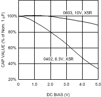 Figure 11. Typical Variation in Capacitance vs DC Bias
The ceramic capacitor’s capacitance can vary with temperature. The capacitor type X7R, which operates over a temperature range of –55°C to 125°C, will only vary the capacitance to within ±15%. The capacitor type X5R has a similar tolerance over a reduced temperature range of –55°C to 85°C. Many large value ceramic capacitors, larger than 1 µF are manufactured with Z5U or Y5V temperature characteristics. Their capacitance can drop by more than 50% as the temperature varies from 25°C to 85°C. Therefore X7R is recommended over Z5U and Y5V in applications where the ambient temperature will change significantly above or below 25°C.
Tantalum capacitors are less desirable than ceramic for use as output capacitors because they are more expensive when comparing equivalent capacitance and voltage ratings in the 1-µF to 4.7-µF range.
Another important consideration is that tantalum capacitors have higher ESR values than equivalent size ceramics. This means that while it may be possible to find a tantalum capacitor with an ESR value within the stable range, it would have to be larger in capacitance (which means bigger and more costly) than a ceramic capacitor with the same ESR value. It should also be noted that the ESR of a typical tantalum will increase about 2:1 as the temperature goes from 25°C down to -40°C, so some guard band must be allowed.
Table 2. Suggested Capacitors and Their Suppliers
| CAPACITANCE / µF | MODEL | VENDOR | TYPE | CASE SIZE / INCH (mm) |
|---|---|---|---|---|
| 1 | C1608X5R1A105K | TDK | Ceramic, X5R | 0603 (1608) |
| 1 | C1005X5R1A105K | TDK | Ceramic, X5R | 0402 (1005) |
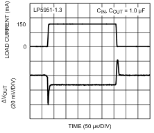
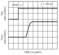
8.2.3 Application Curves