SBOSAA7 September 2025 OPA598
PRODUCTION DATA
- 1
- 1 Features
- 2 Applications
- 3 Description
- 4 Pin Configuration and Functions
- 5 Specifications
- 6 Detailed Description
- 7 Application and Implementation
- 8 Device and Documentation Support
- 9 Revision History
- 10Mechanical, Packaging, and Orderable Information
Package Options
Mechanical Data (Package|Pins)
- DNT|12
Thermal pad, mechanical data (Package|Pins)
Orderable Information
4 Pin Configuration and Functions
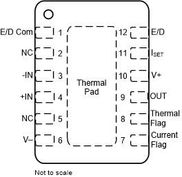
 Figure 4-1 DNT Package, 12-Pin WSON (Top View)
Table 4-1 Pin Functions
| PIN | TYPE | DESCRIPTION | |
|---|---|---|---|
| NAME | NO. | ||
| Current Flag | 7 | Output | Overcurrent status flag |
| E/D | 12 | Input | Enable and disable |
| E/D Com | 1 | Input | Enable and disable common |
| –IN | 3 | Input | Inverting input |
| +IN | 4 | Input | Noninverting input |
| ISET | 11 | — | Current limit |
| NC | 2, 5 | — | No internal connection |
| OUT | 9 | Output | Output |
| Thermal Flag | 8 | Output | Overtemperature status flag |
| Thermal Pad | — | — | The thermal pad is internally connected to V–. The thermal pad must be soldered to a printed-circuit board (PCB) connected to V–, even with applications that have low power dissipation. |
| V– | 6 | Power | Negative (lowest) power supply |
| V+ | 10 | Power | Positive (highest) power supply |