SLES102B December 2003 – March 2015 PCM1798
PRODUCTION DATA.
- 1 Features
- 2 Applications
- 3 Description
- 4 Revision History
- 5 Pin Configuration and Functions
- 6 Specifications
- 7 Detailed Description
- 8 Application and Implementation
- 9 Power Supply Recommendations
- 10Layout
- 11Device and Documentation Support
- 12Mechanical, Packaging, and Orderable Information
Package Options
Refer to the PDF data sheet for device specific package drawings
Mechanical Data (Package|Pins)
- DB|28
Thermal pad, mechanical data (Package|Pins)
Orderable Information
8 Application and Implementation
NOTE
Information in the following applications sections is not part of the TI component specification, and TI does not warrant its accuracy or completeness. TI’s customers are responsible for determining suitability of components for their purposes. Customers should validate and test their design implementation to confirm system functionality.
8.1 Application Information
The PCM1798 device is a hardware-controlled, differential current output DAC that can accept multiple formats of 16- or 24-bit PCM audio data. Because the PCM1798 is a current output part, in most cases a current to voltage stage is required before the signal is passed to the amplifier stage. A microcontroller or DSP can use GPIO to manipulate the control pins CHSL, DEM, FMT0, FMT1, MONO, and MUTE. The PCM1798 requires a 5-V analog supply, as well as a 3.3-V digital supply.
8.2 Typical Applications
8.2.1 Application for External Digital Filter Interface
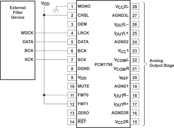 Figure 26. Connection Diagram for External Digital Filter (Internal DF Bypass Mode) Application
8.2.1.1 Design Requirements
- Control: Host controller with SPI communication
- Audio Output: I/V output circuitry
- Audio Input: Digital Audio Filter with I2S or DSD output
8.2.1.2 Detailed Design Procedure
8.2.1.2.1 Application for Interfacing With an External Digital Filter
For some applications, it may be desirable to use a programmable digital signal processor as an external digital filter to perform the interpolation function. The following pin settings enable the external digital filter application mode.
- MONO (pin 1) = LOW
- CHSL (pin 2) = HIGH
- FMT0 (pin 11) = HIGH
- FMT1 (pin 12) = HIGH
The pins used to provide the serial interface for the external digital filter are shown in the connection diagram of Figure 26. The word clock (WDCK) must be operated at 8× or 4× the desired sampling frequency, fS.
Pin assignment when using the external digital filter interface:
- LRCK (pin 4): WDCK as word clock input
- DATA (pin 5): Monaural audio data input
- BCK (pin 6): Bit clock input
8.2.1.2.2 Audio Format
The PCM1798 in the external digital filter interface mode supports the 24-bit right-justified audio format as shown in Figure 27.
 Figure 27. Audio Data Input Format for External Digital Filter (Internal DF Bypass Mode) Application
8.2.1.2.3 Analog Output
Table 3 and Figure 28 show the relationship between the digital input code and analog output.
Table 3. Analog Output Current and Voltage(1)
| 800000 (–FS) | 000000 (BPZ) | 7FFFFF (+FS) | |
|---|---|---|---|
| IOUTN [mA] | –1.5 | –3.5 | –5.5 |
| IOUTP [mA] | –5.5 | –3.5 | –1.5 |
| VOUTN [V] | –1.23 | –2.87 | –4.51 |
| VOUTP [V] | –4.51 | –2.87 | –1.23 |
| VOUT [V] | –2.98 | 0 | 2.98 |
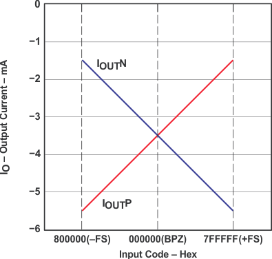 Figure 28. Relationship Between Digital Input and Analog Output
8.2.1.3 Application Curves
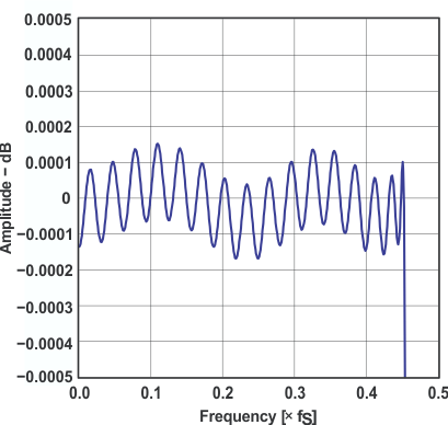
| Pass-Band Ripple, Sharp Rolloff | ||
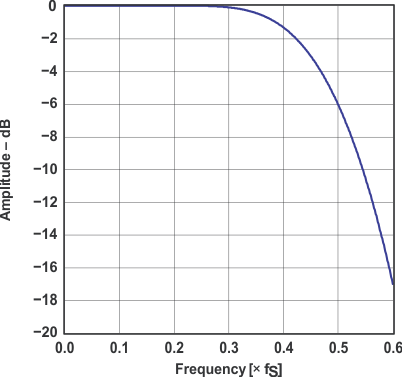
| Transition Characteristics, Slow Rolloff | ||
8.2.2 PCM1798 Typical Application
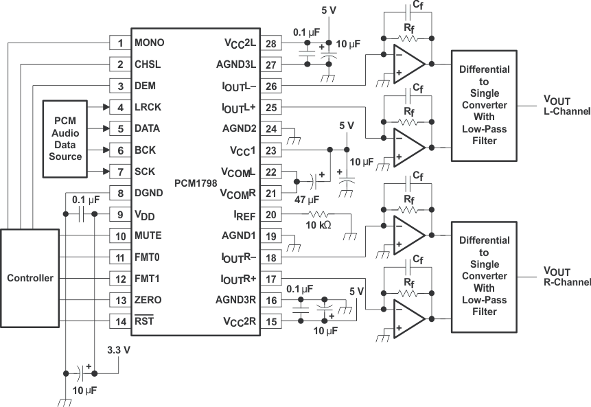 Figure 31. Typical Application Circuit
8.2.2.1 Design Requirements
The design of the application circuit is very important in order to actually realize the high S/N ratio of which the PCM1798 is capable. This is because noise and distortion that are generated in an application circuit are not negligible.
In the third-order LPF circuit of Figure 32, the output level is 2.1 V RMS, and 123 dB S/N is achieved.
8.2.2.2 Detailed Design Procedure
8.2.2.2.1 I/V Section
The current of the PCM1798 on each of the output pins (IOUTL+, IOUTL–, IOUTR+, IOUTR–) is 4 mA p-p at 0 dB (full scale). The voltage output level of the I/V converter (Vi) is given by following equation:
TI recommends an NE5534 operational amplifier for the I/V circuit to obtain the specified performance. Dynamic performance such as the gain bandwidth, settling time, and slew rate of the operational amplifier affects the audio dynamic performance of the I/V section.
8.2.2.2.2 Differential Section
The PCM1798 voltage outputs are followed by differential amplifier stages, which sum the differential signals for each channel, creating a single-ended I/V op-amp output. In addition, the differential amplifiers provide a low-pass filter function.
The operational amplifier recommended for the differential circuit is the low-noise type.
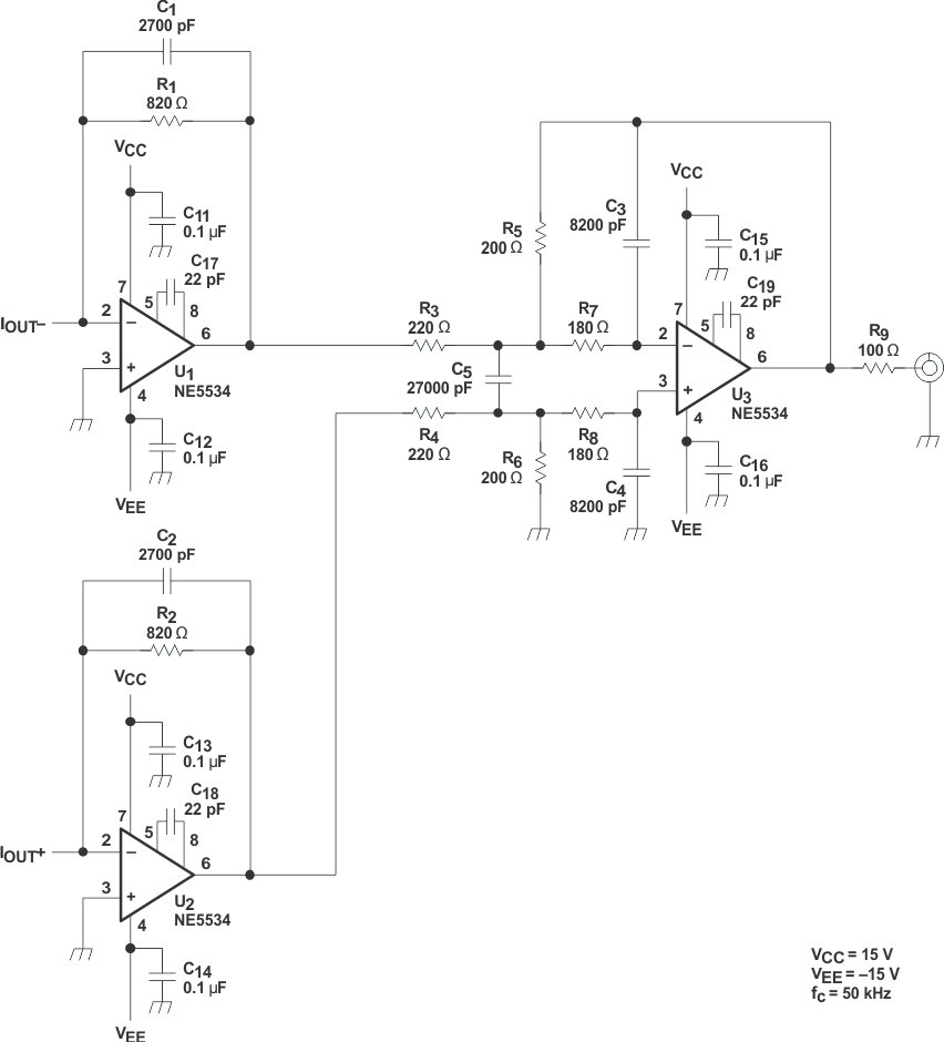 Figure 32. Measurement Circuit
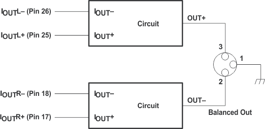 Figure 33. Measurement Circuit for Monaural Mode