SLES102B December   2003  – March 2015 PCM1798

PRODUCTION DATA.  

  1. Features
  2. Applications
  3. Description
  4. Revision History
  5. Pin Configuration and Functions
  6. Specifications
    1. 6.1 Absolute Maximum Ratings
    2. 6.2 ESD Ratings
    3. 6.3 Recommended Operating Conditions
    4. 6.4 Thermal Information
    5. 6.5 Electrical Characteristics
    6. 6.6 Timing Requirements
    7. 6.7 Typical Characteristics for Digital Filter
      1. 6.7.1 Analog Dynamic Performance
  7. Detailed Description
    1. 7.1 Overview
    2. 7.2 Functional Block Diagram
    3. 7.3 Feature Description
      1. 7.3.1 System Clock and Reset Functions
        1. 7.3.1.1 System Clock Input
      2. 7.3.2 Power-On and External Reset Functions
      3. 7.3.3 Audio Data Interface
        1. 7.3.3.1 Audio Serial Interface
        2. 7.3.3.2 PCM Audio Data Formats and Timing
      4. 7.3.4 Function Descriptions
        1. 7.3.4.1 Audio Data Format
        2. 7.3.4.2 Soft Mute
        3. 7.3.4.3 De-Emphasis
        4. 7.3.4.4 Zero Detection
    4. 7.4 Device Functional Modes
  8. Application and Implementation
    1. 8.1 Application Information
    2. 8.2 Typical Applications
      1. 8.2.1 Application for External Digital Filter Interface
        1. 8.2.1.1 Design Requirements
        2. 8.2.1.2 Detailed Design Procedure
          1. 8.2.1.2.1 Application for Interfacing With an External Digital Filter
          2. 8.2.1.2.2 Audio Format
          3. 8.2.1.2.3 Analog Output
        3. 8.2.1.3 Application Curves
      2. 8.2.2 PCM1798 Typical Application
        1. 8.2.2.1 Design Requirements
        2. 8.2.2.2 Detailed Design Procedure
          1. 8.2.2.2.1 I/V Section
          2. 8.2.2.2.2 Differential Section
  9. Power Supply Recommendations
  10. 10Layout
    1. 10.1 Layout Guidelines
    2. 10.2 Layout Example
  11. 11Device and Documentation Support
    1. 11.1 Trademarks
    2. 11.2 Electrostatic Discharge Caution
    3. 11.3 Glossary
  12. 12Mechanical, Packaging, and Orderable Information

Package Options

Refer to the PDF data sheet for device specific package drawings

Mechanical Data (Package|Pins)
  • DB|28
Thermal pad, mechanical data (Package|Pins)
Orderable Information

10 Layout

10.1 Layout Guidelines

Designers should try to use the same ground between AGND and DGND to avoid any potential voltage difference between them. Ensure that the return currents for digital signals will avoid the AGND pin or the input signals to the I/V stage. Avoid running high frequency clock and control signals near AGND, or any of the Vout pins where possible. The pin layout of the PCM1798 partitions into two parts - analog section and digital section. Providing the system is partitioned in such a way that digital signals are routed away from the analog sections, then no digital return currents (for example, clocks) should be generated in the analog circuitry.

  • Decoupling capacitors should be placed as close to the VCC1, VCC2L, VCCR2, VCOML, VCOMR, and VDD pins as possible.
  • Further guidelines can be found in Figure 34.

10.2 Layout Example
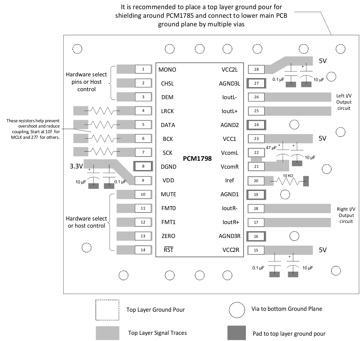
PCM1798 layoutex_SLES102.gifFigure 34. PCM1785 Layout Example