SLES102B December 2003 – March 2015 PCM1798
PRODUCTION DATA.
- 1 Features
- 2 Applications
- 3 Description
- 4 Revision History
- 5 Pin Configuration and Functions
- 6 Specifications
- 7 Detailed Description
- 8 Application and Implementation
- 9 Power Supply Recommendations
- 10Layout
- 11Device and Documentation Support
- 12Mechanical, Packaging, and Orderable Information
Package Options
Refer to the PDF data sheet for device specific package drawings
Mechanical Data (Package|Pins)
- DB|28
Thermal pad, mechanical data (Package|Pins)
Orderable Information
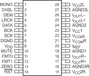
5 Pin Configuration and Functions
DB Package
28-Lead SSOP
Top View

Pin Functions
| PIN | I/O | DESCRIPTION | |
|---|---|---|---|
| NAME | NO. | ||
| AGND1 | 19 | — | Analog ground (internal bias) |
| AGND2 | 24 | — | Analog ground (internal bias) |
| AGND3L | 27 | — | Analog ground (L-channel DACFF) |
| AGND3R | 16 | — | Analog ground (R-channel DACFF) |
| BCK | 6 | Input | Bit clock input(1) |
| CHSL | 2 | Input | L-, R-channel select(1) |
| DATA | 5 | Input | Serial audio data input(1) |
| DEM | 3 | Input | De-emphasis enable(1) |
| DGND | 8 | — | Digital ground |
| FMT0 | 11 | Input | Audio data format select(1) |
| FMT1 | 12 | Input | Audio data format select(1) |
| IOUTL+ | 25 | Output | L-channel analog current output + |
| IOUTL– | 26 | Output | L-channel analog current output – |
| IOUTR+ | 17 | Output | R-channel analog current output + |
| IOUTR– | 18 | Output | R-channel analog current output – |
| IREF | 20 | — | Output current reference bias pin |
| LRCK | 4 | Input | Left and right clock (fS) input(1) |
| MONO | 1 | Input | Monaural mode enable(1) |
| MUTE | 10 | Input | Mute control(1) |
| RST | 14 | Input | Reset(1) |
| SCK | 7 | Input | System clock input(1) |
| VCC1 | 23 | — | Analog power supply, 5 V |
| VCC2L | 28 | — | Analog power supply (L-channel DACFF), 5 V |
| VCC2R | 15 | — | Analog power supply (R-cahnnel DACFF), 5 V |
| VCOML | 22 | — | L-channel internal bias decoupling pin |
| VCOMR | 21 | — | R-channel internal bias decoupling pin |
| VDD | 9 | — | Digital power supply, 3.3 V |
| ZERO | 13 | Output | Zero flag |
(1) Schmitt-trigger input, 5-V tolerant