SLES023D December 2001 – December 2016 PCM1802
PRODUCTION DATA.
- 1 Features
- 2 Applications
- 3 Description
- 4 Revision History
- 5 Pin Configuration and Functions
-
6 Specifications
- 6.1 Absolute Maximum Ratings
- 6.2 ESD Ratings
- 6.3 Recommended Operating Conditions
- 6.4 Thermal Information
- 6.5 Electrical Characteristics
- 6.6 Typical Characteristics
- 7 Detailed Description
- 8 Application and Implementation
- 9 Power Supply Recommendations
- 10Layout
- 11Device and Documentation Support
- 12Mechanical, Packaging, and Orderable Information
Package Options
Mechanical Data (Package|Pins)
- DB|20
Thermal pad, mechanical data (Package|Pins)
Orderable Information
1 Features
- 24-Bit Delta-Sigma Stereo A/D Converter
- Single-Ended Voltage Input: 3 VP–P
- Antialiasing Filter Included
- Oversampling Decimation Filter
- Oversampling Frequency: ×64, ×128
- Pass-Band Ripple: ±0.05 dB
- Stop-Band Attenuation: –65 dB
- On-Chip High-Pass Filter: 0.84 Hz (44.1 kHz)
- High Performance
- THD+N: 96 dB (Typical)
- SNR: 105 dB (Typical)
- Dynamic Range: 105 dB (Typical)
- PCM Audio Interface
- Master and Slave Mode Selectable
- Data Formats: 24-Bit Left-Justified; 24-Bit I2S; 20-bit or 24-Bit Right-Justified
- Sampling Rate: 16 kHz to 96 kHz
- System Clock: 256 fS, 384 fS, 512 fS, 768 fS
- Dual Power Supplies: 5 V (Analog), 3.3 V (Digital)
- Package: 20-Pin SSOP
2 Applications
- AV Amplifier Receivers
- MD Players
- CD Recorders
- Multitrack Receivers
- Electric Musical Instruments
3 Description
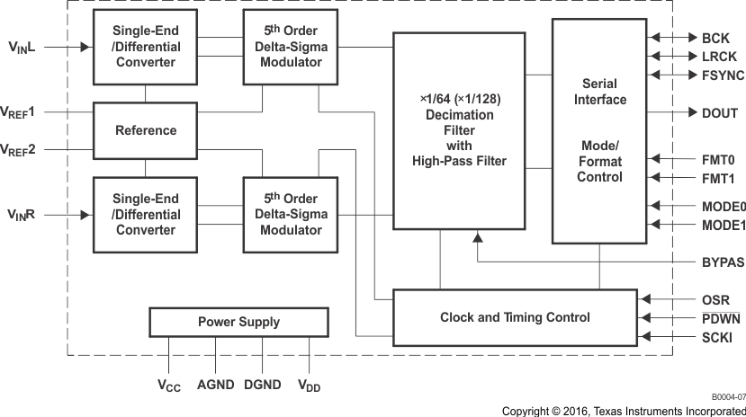
The PCM1802 is a high-performance, low-cost, single-chip stereo analog-to-digital converter with single-ended analog voltage input. The PCM1802 uses a delta-sigma modulator with 64-times or 128‑times oversampling, and includes a digital decimation filter and high-pass filter (HPF), which removes the DC component of the input signal. For various applications, the PCM1802 supports master and slave modes and four data formats in serial interface. The PCM1802 is suitable for a wide variety of cost-sensitive consumer applications where good performance, 5-V analog supply, and 3.3-V digital supply operation is required. The PCM1802 is fabricated using a highly advanced CMOS process and is available in the DB 20-pin SSOP package.
Device Information(1)
| PART NUMBER | PACKAGE | BODY SIZE (NOM) |
|---|---|---|
| PCM1802 | SSOP (20) | 7.20 mm × 5.30 mm |
- For all available packages, see the orderable addendum at the end of the data sheet.
Block Diagram
