SLES023D December 2001 – December 2016 PCM1802
PRODUCTION DATA.
- 1 Features
- 2 Applications
- 3 Description
- 4 Revision History
- 5 Pin Configuration and Functions
-
6 Specifications
- 6.1 Absolute Maximum Ratings
- 6.2 ESD Ratings
- 6.3 Recommended Operating Conditions
- 6.4 Thermal Information
- 6.5 Electrical Characteristics
- 6.6 Typical Characteristics
- 7 Detailed Description
- 8 Application and Implementation
- 9 Power Supply Recommendations
- 10Layout
- 11Device and Documentation Support
- 12Mechanical, Packaging, and Orderable Information
Package Options
Mechanical Data (Package|Pins)
- DB|20
Thermal pad, mechanical data (Package|Pins)
Orderable Information
7 Detailed Description
7.1 Overview
The PCM1802 device consists of a reference circuit, two channels of single-ended-to-differential converter, a fifth-order delta-sigma modulator with full differential architecture, a decimation filter with high-pass filter, and a serial interface circuit. Figure 19 illustrates the total architecture of the PCM1802, Figure 20 illustrates the architecture of single-ended-to-differential converter and antialiasing filter, and Figure 21 is the block diagram of the fifth-order delta-sigma modulator and transfer function. An on-chip high-precision reference with one external capacitor provides all reference voltages that are required by the PCM1802 device and defines the full-scale voltage range for both channels. On-chip single-ended-to-differential signal converters save the design, space, and extra parts cost for external signal converters. Full-differential architecture provides a wide dynamic range and excellent power-supply rejection performance. The input signal is sampled at a ×64 or ×128 oversampling rate, thus eliminating an external sample-hold amplifier. A fifth-order delta-sigma noise shaper, which consists of five integrators using the switched capacitor technique and a comparator, shapes the quantization noise generated by the comparator and 1-bit DAC outside of the audio signal band. The high-order delta-sigma modulation randomizes the modulator outputs and reduces the idle tone level. The 64-fS or 128-fS, 1-bit stream from the delta-sigma modulator is converted to a 1-fS, 24-bit or 20-bit digital signal by removing high-frequency noise components with a decimation filter. The DC component of the signal is removed by the HPF, and the HPF output is converted to a time-multiplexed serial signal through the serial interface, which provides flexible serial formats.
7.2 Functional Block Diagrams
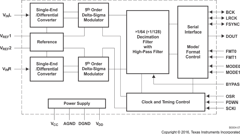 Figure 19. Block Diagram
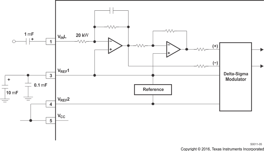 Figure 20. Analog Front End (Left Channel)
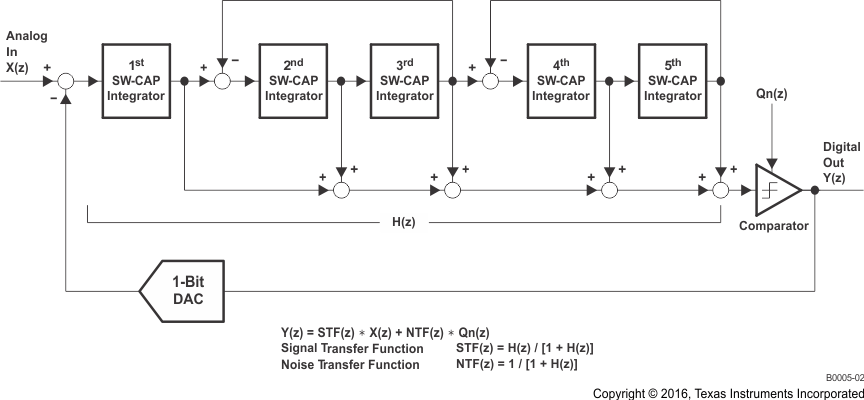 Figure 21. Block Diagram of Fifth-Order Delta-Sigma Modulator
7.3 Feature Description
7.3.1 Hardware Control
The FMT0, FMT1, OSR, BYPASS, MD0, and MD1 pins allow the device to be controlled by tying these pins to GPIO and GND or VDD from a host IC. These controls allow full configuration of the PCM1802.
7.3.2 Power-On Reset Sequence
The PCM1802 has an internal power-on reset circuit, and initialization (reset) is performed automatically when the power supply (VDD) exceeds 2.2 V (typical). While VDD < 2.2 V (typical), and for 1024 system-clock counts after VDD > 2.2 V (typical), the PCM1802 stays in the reset state and the digital output is forced to zero. The digital output is valid after the reset state is released and the time of 4480 / fS is passed. Figure 22 illustrates the internal power-on reset timing and the digital output for power-on reset.
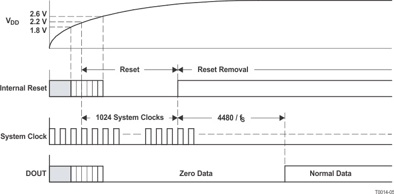 Figure 22. Internal Power-On Reset Timing
7.3.3 System Clock
The PCM1802 supports 256 fS, 384 fS, 512 fS, and 768 fS as the system clock, where fS is the audio sampling frequency. The system clock must be supplied on SCKI.
The PCM1802 has a system clock detection circuit which automatically senses if the system clock is operating at 256 fS, 384 fS, 512 fS, or 768 fS in slave mode. In master mode, the system clock frequency must be selected by MODE0 and MODE1, and 768 fS is not available. For system clock inputs of 384 fS, 512 fS, and 768 fS, the system clock is divided to 256 fS automatically, and the 256 fS clock operates the delta-sigma modulator and the digital filter.
Table 1 lists the relationship of typical sampling frequencies and system clock frequencies, and Table 2 shows system clock timing.
Table 1. Sampling Frequency and System Clock Frequency
| SAMPLING RATE FREQUENCY (kHz) |
SYSTEM CLOCK FREQUENCY (MHz) | |||
|---|---|---|---|---|
| 256 fS | 384 fS | 512 fS | 768 fS | |
| 32 | 8.192 | 12.288 | 16.384 | 24.576 |
| 44.1 | 11.2896 | 16.9344 | 22.5792 | 33.8688 |
| 48 | 12.288 | 18.432 | 24.576 | 36.864 |
| 64 | 16.384 | 24.576 | 32.768 | 49.152 |
| 88.2 | 22.5792 | 33.8688 | 45.1584 | — |
| 96 | 24.576 | 36.864 | 49.152 | — |

Table 2. System Clock Timing
| PARAMETER | MIN | MAX | UNIT | |
|---|---|---|---|---|
| tw(SCKH) | System clock-pulse duration, high | 7 | ns | |
| tw(SCKL) | System clock-pulse duration, low | 7 | ns | |
7.4 Device Functional Modes
7.4.1 Power Down, HPF Bypass, Oversampling Control
PDWN controls the entire ADC operation. During power-down mode, both the supply current for the analog portion and the clock signal for the digital portion are shut down, and power dissipation is minimized. DOUT is also disabled and no system clock is accepted during power-down mode.
Table 3. Power-Down Control
| PDWN | MODE |
|---|---|
| LOW | Power-down mode |
| HIGH | Normal operation mode |
The built-in function for DC component rejection can be bypassed using the BYPAS control. In bypass mode, the DC components of the analog input signal, such as the internal DC offset, are converted and included in the digital output data.
Table 4. HPF Bypass Control
| BYPAS | HPF (HIGH-PASS FILTER) MODE |
|---|---|
| LOW | Normal (no DC component on DOUT) mode |
| HIGH | Bypass (DC component on DOUT) mode |
OSR controls the oversampling ratio of the delta-sigma modulator, ×64 or ×128. The ×128 mode is available for fS < 50 kHz, and must be used carefully as the duty cycle of the 384 fS system clock affects performance.
Table 5. Oversampling Control
| OSR | OVERSAMPLING RATIO |
|---|---|
| LOW | ×64 |
| HIGH | ×128 (fS < 50 kHz) |
7.4.2 Serial Audio Data Interface
The PCM1802 interfaces with the audio system through BCK, LRCK, FSYNC, and DOUT.
7.4.2.1 Data Format
The PCM1802 supports four audio data formats in both master and slave modes, and they are selected by FMT1 and FMT0 as shown in Table 6. Figure 23 and Figure 25 illustrate the data formats in slave mode and master mode, respectively.
Table 6. Data Format
| FORMAT | FMT1 | FMT0 | FORMAT |
|---|---|---|---|
| 0 | 0 | 0 | Left-justified, 24-bit |
| 1 | 0 | 1 | I2S, 24-bit |
| 2 | 1 | 0 | Right-justified, 24-bit |
| 3 | 1 | 1 | Right-justified, 20-bit |
7.4.2.2 Interface Timing
Figure 24 and Figure 26 illustrate the interface timing in slave mode and master mode, respectively.
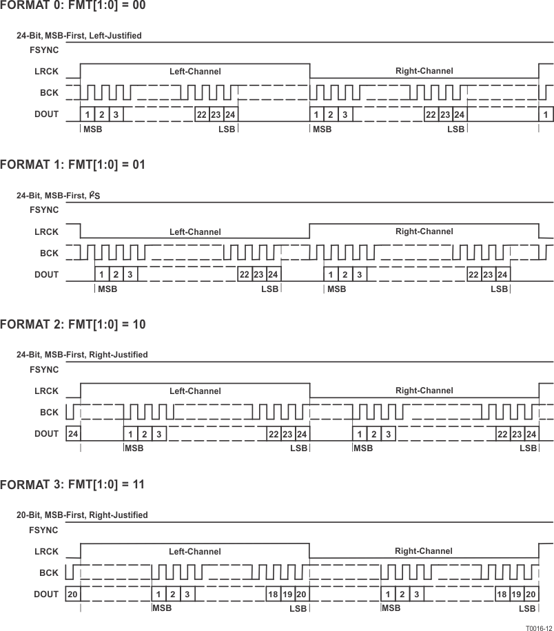 Figure 23. Audio Data Format (Slave Mode: FSYNC, LRCK, and BCK Work as Inputs)
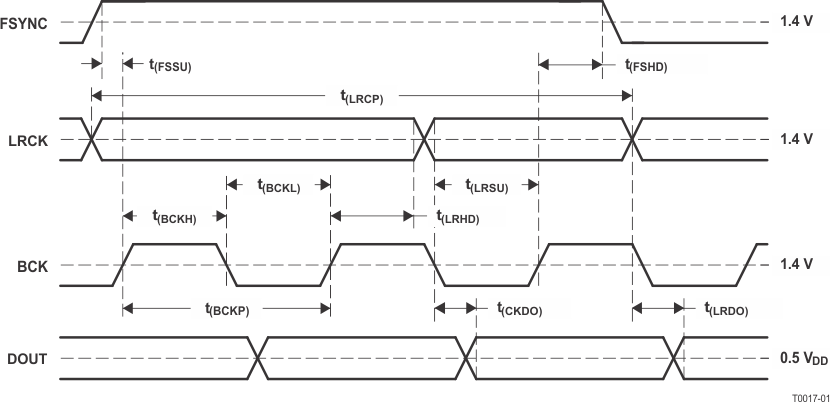
Table 7. Audio Data Interface Timing: Slave Mode
| PARAMETER | MIN | MAX | UNIT | |
|---|---|---|---|---|
| t(BCKP) | BCK period | 150 | ns | |
| t(BCKH) | BCK pulse duration, high | 60 | ns | |
| t(BCKL) | BCK pulse duration, low | 60 | ns | |
| t(LRSU) | LRCK setup time to BCK rising edge | 40 | ns | |
| t(LRHD) | LRCK hold time to BCK rising edge | 20 | ns | |
| t(LRCP) | LRCK period | 10 | µs | |
| t(FSSU) | FSYNC setup time to BCK rising edge | 20 | ns | |
| t(FSHD) | FSYNC hold time to BCK rising edge | 20 | ns | |
| t(CKDO) | Delay time, BCK falling edge to DOUT valid | –10 | 20 | ns |
| t(LRDO) | Delay time, LRCK edge to DOUT valid | –10 | 20 | ns |
| tr | Rise time of all signals | 10 | ns | |
| tf | Fall time of all signals | 10 | ns | |
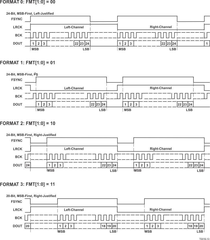 Figure 25. Audio Data Format (Master Mode: FSYNC, LRCK, and BCK Work as Outputs)
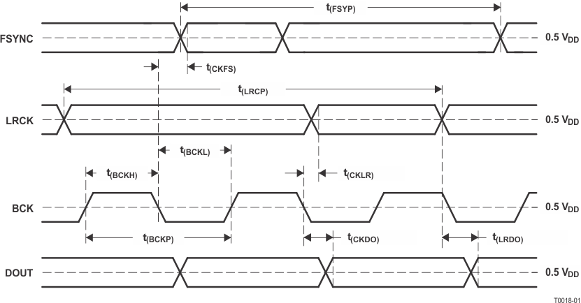
Table 8. Audio Data Interface Timing: Master Mode
| PARAMETER | MIN | TYP | MAX | UNIT | |
|---|---|---|---|---|---|
| t(BCKP) | BCK period | 150 | 1 / (64 fS) | 1200 | ns |
| t(BCKH) | BCK pulse duration, high | 75 | 600 | ns | |
| t(BCKL) | BCK pulse duration, low | 75 | 600 | ns | |
| t(CKLR) | Delay time, BCK falling edge to LRCK valid | –10 | 20 | ns | |
| t(LRCP) | LRCK period | 10 | 1 / fS | 80 | µs |
| t(CKFS) | Delay time, BCK falling edge to FSYNC valid | –10 | 20 | ns | |
| t(FSYP) | FSYNC period | 5 | 1 / (2 fS) | 40 | µs |
| t(CKDO) | Delay time, BCK falling edge to DOUT valid | –10 | 20 | ns | |
| t(LRDO) | Delay time, LRCK edge to DOUT valid | –10 | 20 | ns | |
| tr | Rise time of all signals | 10 | ns | ||
| tf | Fall time of all signals | 10 | ns | ||
7.4.2.3 Synchronization With Digital Audio System
In slave mode, the PCM1802 operates under LRCK, synchronized with system clock SCKI. The PCM1802 does not require a specific phase relationship between LRCK and SCKI, but does require the synchronization of LRCK and SCKI.
If the relationship between LRCK and SCKI changes more than ±6 BCKs for 64 fS BCK (±5 BCKs for 48 fS BCK) during one sample period due to LRCK or SCKI jitter, internal operation of the ADC halts within 1 / fS and digital output is forced into BPZ code until resynchronization between LRCK and SCKI is completed.
In the case of changes less than ±5 BCKs for 64 BCK per frame (±4 BCKs for 48 BCK per frame), resynchronization does not occur.
Figure 27 illustrates the digital output response for loss of synchronization and resynchronization. During undefined data, some noise might be generated in the audio signal. The transition of normal to undefined data and undefined or zero data to normal creates a data discontinuity in the digital output, which generates some noise in the audio signal.
TI recommends setting PDWN low to achieve stable analog performance when the sampling rate, interface mode, data format, or oversampling control is changed.
 Figure 27. ADC Digital Output for Loss of Synchronization and Resynchronization
7.4.3 Master Mode
In master mode, BCK, LRCK, and FSYNC work as output pins, and these pins are controlled by timing which is generated in the clock circuit of the PCM1802. FSYNC is used to designate the valid data from the PCM1802. The rising edge of FSYNC indicates the starting point of the converted audio data and the falling edge of this signal indicates the ending point of the data. The frequency of this signal is fixed at 2 × LRCK. The duty cycle ratio depends on data bit length. The frequency of BCK is fixed at 64 × LRCK. The 768-fS system clock is not available in master mode.
7.4.4 Slave Mode
In slave mode, BCK, LRCK, and FSYNC work as input pins. FSYNC enables the BCK signal, and the device can shift out the converted data while FSYNC is HIGH. The PCM1802 accepts the 64-fS BCK or the 48-fS BCK format. The delay of FSYNC from the LRCK transition must be within 16 BCKs for the 64-fS BCK format and within 12 BCKs for the 48-fS BCK format.
7.4.5 Interface Mode
The PCM1802 supports master mode and slave mode as interface modes, and they are selected by MODE1 and MODE0 as shown in Table 9.
In master mode, the PCM1802 provides the timing for serial audio data communications between the PCM1802 and the digital audio processor or external circuit. In slave mode, the PCM1802 receives the timing for data transfer from an external controller.
Table 9. Interface Mode
| MODE1 | MODE0 | INTERFACE MODE |
|---|---|---|
| 0 | 0 | Slave mode (256 fS, 384 fS, 512 fS, 768 fS) |
| 0 | 1 | Master mode (512 fS) |
| 1 | 0 | Master mode (384 fS) |
| 1 | 1 | Master mode (256 fS) |