SNAS781G October 2020 – September 2023 REF70
PRODMIX
- 1
- 1 Features
- 2 Applications
- 3 Description
- 4 Revision History
- 5 Device Comparison Table
- 6 Pin Configuration and Functions
-
7 Specifications
- 7.1 Absolute Maximum Ratings
- 7.2 ESD Ratings
- 7.3 Recommended Operating Conditions
- 7.4 Thermal Information
- 7.5 REF7012 Electrical Characteristics
- 7.6 REF7025 Electrical Characteristics
- 7.7 REF7030 Electrical Characteristics
- 7.8 REF7033 Electrical Characteristics
- 7.9 REF7040 Electrical Characteristics
- 7.10 REF7050 Electrical Characteristics
- 7.11 Typical Characteristics
- 8 Parameter Measurement Information
- 9 Detailed Description
- 10Application and Implementation
- 11Device and Documentation Support
- 12Mechanical, Packaging, and Orderable Information
Package Options
Mechanical Data (Package|Pins)
Thermal pad, mechanical data (Package|Pins)
Orderable Information
8.5 Temperature Drift
The REF70 is designed and tested for a minimal output voltage temperature drift, which is defined as the change in output voltage over temperature. Every unit shipped is tested at multiple temperatures to ensure that the product meets data sheet specifications. The temperature coefficient is calculated using the box method in which a box is formed by the min/max limits for the nominal output voltage over the operating temperature range. REF70 has a low maximum temperature coefficient of 2 ppm/°C from –40°C to +125°C. This method corresponds more accurately to the method of test and provides a closer estimate of actual error than the other methods. The box method specifies limits for the temperature error but does not specify the exact shape and slope of the device under test. Due to temperature curvature correction to achieve low-temperature drift, the temperature drift is expected to be non-linear. See SLYT183 for more information on the box method. The box method equation is shown in Equation 2:
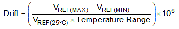
 Figure 8-14 Output Voltage Vs Free-Air Temperature