SNAS781G October 2020 – September 2023 REF70
PRODMIX
- 1
- 1 Features
- 2 Applications
- 3 Description
- 4 Revision History
- 5 Device Comparison Table
- 6 Pin Configuration and Functions
-
7 Specifications
- 7.1 Absolute Maximum Ratings
- 7.2 ESD Ratings
- 7.3 Recommended Operating Conditions
- 7.4 Thermal Information
- 7.5 REF7012 Electrical Characteristics
- 7.6 REF7025 Electrical Characteristics
- 7.7 REF7030 Electrical Characteristics
- 7.8 REF7033 Electrical Characteristics
- 7.9 REF7040 Electrical Characteristics
- 7.10 REF7050 Electrical Characteristics
- 7.11 Typical Characteristics
- 8 Parameter Measurement Information
- 9 Detailed Description
- 10Application and Implementation
- 11Device and Documentation Support
- 12Mechanical, Packaging, and Orderable Information
Package Options
Mechanical Data (Package|Pins)
Thermal pad, mechanical data (Package|Pins)
Orderable Information
3 Description
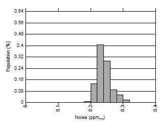
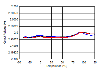
The REF70 is a family of high precision series voltage references that offers the industry’s lowest noise (0.23 ppmp-p), very low temperature drift coefficient (2 ppm/°C), and high accuracy (±0.025%). The REF70 offers a high PSRR, low drop-out voltage and excellent load and line regulation to help meet strict transient requirements. This combination of precision and features is designed for applications such as test and measurement that demand a precise reference to be paired with precision, high-resolution data converters such as ADS8900B, ADS127L01 and DAC11001A, to achieve optimal performance in the signal chain. The REF70 is also designed for noise-sensitive medical applications such as ultrasound and X-ray to help enable low-noise measurements from the analog front end.
The REF70 family is available in VSSOP and LCCC package options. The LCCC (FKH) package is a hermetically sealed ceramic package that allows for low, long-term drift for applications that require a stable reference over a long time period without calibration.
The REF70 is specified for the wide temperature range of −40°C to +125°C. The wide temperature range enables operation across various industrial applications.
| PART NAME | PACKAGE (1) | BODY SIZE (NOM) |
|---|---|---|
| REF70 | LCCC (8) | 5.00 mm × 5.00 mm |
| VSSOP (8) | 3.00 mm x 3.00 mm |
 0.1-Hz to 10-Hz Voltage Noise Distribution
 Output Voltage Vs Free-Air-Temperature