SNAS781G October 2020 – September 2023 REF70
PRODMIX
- 1
- 1 Features
- 2 Applications
- 3 Description
- 4 Revision History
- 5 Device Comparison Table
- 6 Pin Configuration and Functions
-
7 Specifications
- 7.1 Absolute Maximum Ratings
- 7.2 ESD Ratings
- 7.3 Recommended Operating Conditions
- 7.4 Thermal Information
- 7.5 REF7012 Electrical Characteristics
- 7.6 REF7025 Electrical Characteristics
- 7.7 REF7030 Electrical Characteristics
- 7.8 REF7033 Electrical Characteristics
- 7.9 REF7040 Electrical Characteristics
- 7.10 REF7050 Electrical Characteristics
- 7.11 Typical Characteristics
- 8 Parameter Measurement Information
- 9 Detailed Description
- 10Application and Implementation
- 11Device and Documentation Support
- 12Mechanical, Packaging, and Orderable Information
Package Options
Mechanical Data (Package|Pins)
Thermal pad, mechanical data (Package|Pins)
Orderable Information
8.3 Thermal Hysteresis
Thermal hysteresis is measured with the REF70 soldered to a PCB, similar to a real-world application. Thermal hysteresis for the device is defined as the change in output voltage after operating the device at 25°C, cycling the device through the specified temperature range, and returning to 25°C. This can be seen in Figure 8-6 to Figure 8-8. Hysteresis can be expressed by Equation 1:
Equation 1. 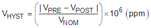
where
- VHYST = thermal hysteresis (in units of ppm)
- VNOM = the specified output voltage
- VPRE = output voltage measured at 25°C pre-temperature cycling
- VPOST = output voltage measured after the device has cycled from 25°C through the specified temperature range of –40°C to +125°C and returns to 25°C.
") Figure 8-6 REF7025QFKHR Thermal
Hysteresis Distribution (-40°C to 125°C)
Figure 8-6 REF7025QFKHR Thermal
Hysteresis Distribution (-40°C to 125°C)") Figure 8-8 REF7012QFKHR Thermal
Hysteresis Distribution (-40°C to 125°C)
Figure 8-8 REF7012QFKHR Thermal
Hysteresis Distribution (-40°C to 125°C)") Figure 8-7 REF7012QDGKR Thermal
Hysteresis Distribution (-40°C to 125°C)
Figure 8-7 REF7012QDGKR Thermal
Hysteresis Distribution (-40°C to 125°C)