SNAS781G October 2020 – September 2023 REF70
PRODMIX
- 1
- 1 Features
- 2 Applications
- 3 Description
- 4 Revision History
- 5 Device Comparison Table
- 6 Pin Configuration and Functions
-
7 Specifications
- 7.1 Absolute Maximum Ratings
- 7.2 ESD Ratings
- 7.3 Recommended Operating Conditions
- 7.4 Thermal Information
- 7.5 REF7012 Electrical Characteristics
- 7.6 REF7025 Electrical Characteristics
- 7.7 REF7030 Electrical Characteristics
- 7.8 REF7033 Electrical Characteristics
- 7.9 REF7040 Electrical Characteristics
- 7.10 REF7050 Electrical Characteristics
- 7.11 Typical Characteristics
- 8 Parameter Measurement Information
- 9 Detailed Description
- 10Application and Implementation
- 11Device and Documentation Support
- 12Mechanical, Packaging, and Orderable Information
Package Options
Mechanical Data (Package|Pins)
Thermal pad, mechanical data (Package|Pins)
Orderable Information
8.4.2 Broadband Noise
Broadband noise is a noise that appears at
higher frequency compared to 1/f noise. The broadband noise is usually flat
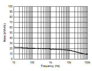
and uniform over frequency as shown in Figure 8-40. The
broadband noise is measured by high-pass filtering the output of the REF70
and measuring the result on a spectrum analyzer as shown in Figure 8-12. The
DC component of the REF70 is removed by using a high-pass filter and then
amplified. When measuring broadband noise, it is not necessary to have high
gain in order to achieve maximum bandwidth.
 Figure 8-12 Broadband
Noise Test Setup
Figure 8-12 Broadband
Noise Test SetupFor noise sensitive designs, a low-pass filter can
be used to reduce broadband noise output noise levels by removing the high
frequency components. When designing a low-pass filter special care must be
taken to ensure the output impedance of the filter does not degrade ac
performance. This can occur in RC low-pass filters where a large series
resistance can impact the load transients due to output current
fluctuations.
 Figure 8-13 Noise
Performance 10 Hz to 100 kHz
 Figure 8-13 Noise
Performance 10 Hz to 100 kHz