SCDS411D July 2019 – October 2022 SN3257-Q1
PRODUCTION DATA
- 1 Features
- 2 Applications
- 3 Description
- 4 Revision History
- 5 Pin Configuration and Functions
- 6 Specifications
-
7 Parameter Measurement Information
- 7.1 On-Resistance
- 7.2 Off-Leakage Current
- 7.3 On-Leakage Current
- 7.4 IPOFF Leakage Current
- 7.5 Transition Time
- 7.6 tON (EN) and tOFF (EN) Time
- 7.7 tON (VDD) and tOFF (VDD) Time
- 7.8 Break-Before-Make Delay
- 7.9 Propagation Delay
- 7.10 Skew
- 7.11 Charge Injection
- 7.12 Capacitance
- 7.13 Off Isolation
- 7.14 Channel-to-Channel Crosstalk
- 7.15 Bandwidth
- 8 Detailed Description
- 9 Application and Implementation
- 10Power Supply Recommendations
- 11Layout
- 12Device and Documentation Support
- 13Mechanical, Packaging, and Orderable Information
Package Options
Mechanical Data (Package|Pins)
Thermal pad, mechanical data (Package|Pins)
Orderable Information
8.4.1 Truth Tables
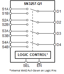
Table 8-1 SN3257-Q1 Truth Table
| INPUTS | Selected Source Pins Connected To Drain Pins (Dx) | |
|---|---|---|
| EN | SEL | |
| 0 | 0 | S1A connected to D1 S2A connected to D2 S3A connected to D3 S4A connected to D4 |
| 0 | 1 | S1B connected to D1 S2B connected to D2 S3B connected to D3 S4B connected to D4 |
| 1 | X(1) | Hi-Z (OFF) |
(1) X denotes do not care.
 Figure 8-1 SN3257-Q1 Functional Block Diagram