SCDS411D July 2019 – October 2022 SN3257-Q1
PRODUCTION DATA
- 1 Features
- 2 Applications
- 3 Description
- 4 Revision History
- 5 Pin Configuration and Functions
- 6 Specifications
-
7 Parameter Measurement Information
- 7.1 On-Resistance
- 7.2 Off-Leakage Current
- 7.3 On-Leakage Current
- 7.4 IPOFF Leakage Current
- 7.5 Transition Time
- 7.6 tON (EN) and tOFF (EN) Time
- 7.7 tON (VDD) and tOFF (VDD) Time
- 7.8 Break-Before-Make Delay
- 7.9 Propagation Delay
- 7.10 Skew
- 7.11 Charge Injection
- 7.12 Capacitance
- 7.13 Off Isolation
- 7.14 Channel-to-Channel Crosstalk
- 7.15 Bandwidth
- 8 Detailed Description
- 9 Application and Implementation
- 10Power Supply Recommendations
- 11Layout
- 12Device and Documentation Support
- 13Mechanical, Packaging, and Orderable Information
Package Options
Mechanical Data (Package|Pins)
Thermal pad, mechanical data (Package|Pins)
Orderable Information
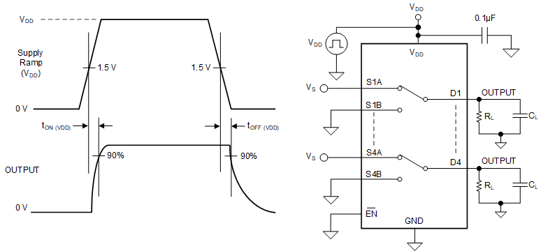
7.7 tON (VDD) and tOFF (VDD) Time
The tON (VDD) time is defined as the time taken by the output of the device to rise to 90% after the supply has risen past the supply threshold. The 90% measurement is used to provide the timing of the device turning on in the system. Figure 7-7 shows the setup used to measure turn on time, denoted by the symbol tON (VDD).
The tOFF (VDD) time is defined as the time taken by the output of the device to fall to 90% after the supply has fallen past the supply threshold. The 90% measurement is used to provide the timing of the device turning off in the system. Figure 7-7 shows the setup used to measure turn off time, denoted by the symbol tOFF (VDD).
 Figure 7-7 tON (VDD) and
tOFF (VDD) Time Measurement Setup