SLLS301R APRIL 1998 – January 2016 SN65LVDS050 , SN65LVDS051 , SN65LVDS179 , SN65LVDS180
PRODUCTION DATA.
- 1 Features
- 2 Applications
- 3 Description
- 4 Revision History
- 5 Description (Continued)
- 6 Device Options
- 7 Pin Configuration and Functions
-
8 Specifications
- 8.1 Absolute Maximum Ratings
- 8.2 ESD Ratings
- 8.3 Recommended Operating Conditions
- 8.4 Thermal Information
- 8.5 Device Electrical Characteristics
- 8.6 Driver Electrical Characteristics
- 8.7 Receiver Electrical Characteristics
- 8.8 Driver Switching Characteristics
- 8.9 Receiver Switching Characteristics
- 8.10 Typical Characteristics
- 9 Parameter Measurement Information
- 10Detailed Description
- 11Application and Implementation
- 12Power Supply Recommendations
- 13Layout
- 14Device and Documentation Support
- 15Mechanical, Packaging, and Orderable Information
Package Options
Refer to the PDF data sheet for device specific package drawings
Mechanical Data (Package|Pins)
- PW|16
- D|16
Thermal pad, mechanical data (Package|Pins)
Orderable Information
10 Detailed Description
10.1 Overview
The SN65LVDSxxx devices are single- and dual-channel LVDS line drivers and receivers. They operate from a single supply that is nominally 3.3 V, but can be as low as 3.0 V and as high as 3.6 V.
The input signal to the drivers is an LVTTL signal. The output of the drivers is a differential signal complying with the LVDS standard (TIA/EIA-644). The driver differential output signal operates with a signal level of 340 mV, nominally, at a common-mode voltage of 1.2 V. This low differential output voltage results in a low emitted radiated energy, which is dependent on the signal slew rate. The differential nature of the output provides immunity to common-mode coupled signals that the driven signal may experience.
The SN65LVDSxxx devices are intended to drive a 100-Ω transmission line. This transmission line may be a printed-circuit board (PCB) or cabled interconnect. With transmission lines, the optimum signal quality and power delivery is reached when the transmission line is terminated with a load equal to the characteristic impedance of the interconnect. Likewise, the driven 100-Ω transmission line should be terminated with a matched resistance.
The SN65LVDSxxx devices also include LVDS line receivers. The input signal to the receivers is a differential LVDS signal. The output of the device is an LVTTL digital signal. This LVDS receivers require ±50 mV of input signal to determine the correct state of the received signal. Compliant LVDS receivers can accept input signals with a common-mode range between 0.025 V and 2.375 V. As the common-mode output voltage of an LVDS driver is 1.2 V, the SN65LVDSxxx receivers correctly determine the line state when operated with a 1-V ground shift between driver and receiver.
10.2 Functional Block Diagram

10.3 Feature Description
10.3.1 Driver Offset
An LVDS-compliant driver is required to maintain the common-mode output voltage at 1.2 V (±75 mV). The SN65LVDSxxx drivers incorporate sense circuitry and a control loop to source common-mode current and keep the output signal within specified values. Further, the device maintains the output common-mode voltage at this set point over the full 3.0-V to 3.6-V supply range.
10.3.2 5-V Input Tolerance
5-V and 3.3-V TTL logic standards share the same input high-voltage and input low-voltage thresholds, namely 2.0 V and 0.8 V, respectively. Although the maximum supply voltage for the SN65LVDSxxx is 3.6 V, the driver can operate and meet all performance requirements when the input signals are as high as 5 V. This allows operation with 3.3-V TTL as well as 5-V TTL logic. 3.3-V CMOS and 5-V CMOS inputs are also allowable, although one should ensure that the duty-cycle distortion that will result from the TTL (ground-referenced) thresholds are acceptable.
10.3.3 NC Pins
NC (not connected) pins are pins where the die is not physically connected to the lead frame or package. For optimum thermal performance, a good rule of thumb is to ground the NC pins at the board level.
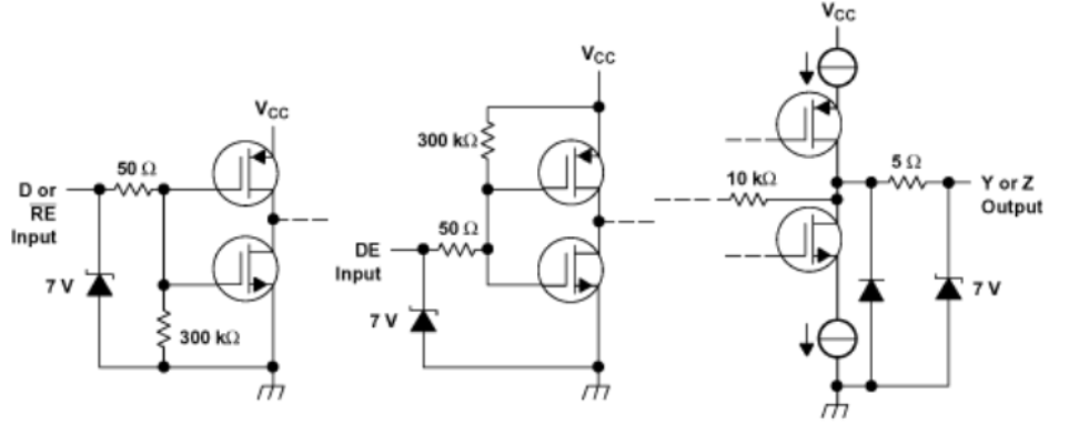
10.3.4 Driver Equivalent Schematics
The SN65LVDSxxx equivalent input and output schematic diagrams are shown in Figure 17. The driver input is represented by a CMOS inverter stage with a 7-V Zener diode. The input stage is high-impedance, and includes an internal pulldown to ground. If the driver input is left open, the driver input provides a low-level signal to the rest of the driver circuitry, resulting in a low-level signal at the driver output pins. The Zener diode provides ESD protection. The driver output stage is a differential pair, one half of which is shown in Figure 17. Like the input stage, the driver output includes Zener diodes for ESD protection. The schematic shows an output stage that includes a set of current sources (nominally 3.5 mA) that are connected to the output load circuit based upon the input stage signal. To the first order, the SN65LVDSxxx output stage acts a constant-current source.
 Figure 17. Equivalent Input and Output Schematic Diagrams
10.3.5 Receiver Features
10.3.5.1 Receiver Output States
When the receiver differential input signal is greater than 50 mV, the receiver output is high, and when the differential input voltage is below –50 mV, the receiver output is low. When the input voltage is between these thresholds (for example, between –50 mV and +50 mV), the receiver output is indeterminate. It may be high or low. A special case occurs when the input to the receiver is open-circuited, which is covered in Receiver Open-Circuit Fail-Safe. When the receiver is disabled, the receiver outputs will be high-impedance.
10.3.5.2 Receiver Open-Circuit Fail-Safe
One of the most common problems with differential signaling applications is how the system responds when no differential voltage is present on the signal pair. The LVDS receiver is like most differential line receivers in that its output logic state can be indeterminate when the differential input voltage is between –100 mV and 100 mV and within its recommended input common-mode voltage range. However, the SN65LVDSxxx receiver is different in how it handles the open-input circuit situation.
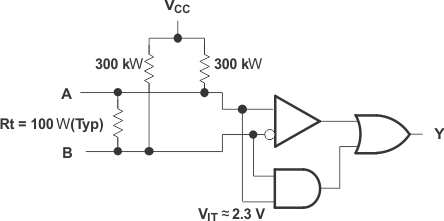
Open circuit means that there is little or no input current to the receiver from the data line itself. This could be when the driver is in a high-impedance state or the cable is disconnected. When this occurs, the LVDS receiver pulls each line of the signal to VCC through 300-kΩ resistors as shown in Figure 18. The fail-safe feature uses an AND gate with input voltage thresholds at about 2.3 V to detect this condition and force the output to a high level.
 Figure 18. Open-Circuit Fail Safe of the LVDS Receiver
It is only under these conditions that the output of the receiver is valid with less than a 100-mV differential input voltage magnitude. The presence of the termination resistor, Rt does not affect the fail-safe function as long as it is connected as shown in Figure 18. Other termination circuits may allow a dc current to ground that could defeat the pullup currents from the receiver and the fail-safe feature.
10.3.5.3 Receiver Power-On Reset
The SN65LVDSxxx receivers include power-on reset circuitry. When the supply voltage drops below 1.5 V (or is turning on and has not yet reached 1.5 V), power-on reset circuitry sets the receiver input pins to a high-impedance state.
10.3.5.4 Common-Mode Range vs Supply Voltage
The SN65LVDSxxx receivers operate over an input common-mode range from VID/2 V to (2.4 – VID/2) V. Hence, if the input signal is a minimum differential voltage of 50 mV, common-mode values in the range of 0.025 V to 2.375 V are supported.
10.3.5.5 General Purpose Comparator
While the SN65LVDSxxx are LVDS standard-compliant receivers, their utility and applications extend to a wider range of signals. As long as the input signals are within the required differential and common-mode voltage ranges mentioned above, the receiver output will be a faithful representation of the input signal.
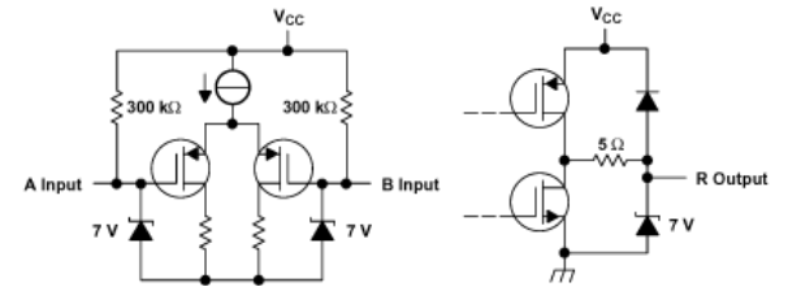
10.3.5.6 Receiver Equivalent Schematics
The SN65LVDSxxx receiver equivalent input and output schematic diagrams are shown in Figure 19. The receiver input is a high-impedance differential pair. 7-V Zener diodes are included on each input to provide ESD protection. The receiver output structure shown is a CMOS inverter with an additional Zener diode, again for ESD protection.
 Figure 19. Equivalent Input and Output Schematic Diagrams
10.4 Device Functional Modes
10.4.1 Function Tables
Table 3. SN65LVDS179 Receiver
| INPUTS | OUTPUT(1) |
|---|---|
| VID = VA – VB | R |
| VID ≥ 100 mV | H |
| –100 mV < VID < 100 mV | ? |
| VID ≤ –100 mV | L |
| Open | H |
Table 4. SN65LVDS179 Driver(1)
| INPUT | OUTPUTS | |
|---|---|---|
| D | Y | Z |
| L | L | H |
| H | H | L |
| Open | L | H |
Table 5. SN65LVDS180, SN65LVDS050, and SN65LVDS051 Receivers(1)
| INPUTS | OUTPUT | |
|---|---|---|
| VID = VA – VB | RE | R |
| VID ≥ 100 mV | L | H |
| –100 mV < VID < 100 mV | L | ? |
| VID ≤ –100 mV | L | L |
| Open | L | H |
| X | H | Z |
? = indeterminate
Table 6. SN65LVDS180, SN65LVDS050, and SN65LVDS051 Drivers(1)
| INPUTS | OUTPUTS | ||
|---|---|---|---|
| D | DE | Y | Z |
| L | H | L | H |
| H | H | H | L |
| Open | H | L | H |
| X | L | Off | Off |