SLLS301R APRIL 1998 – January 2016 SN65LVDS050 , SN65LVDS051 , SN65LVDS179 , SN65LVDS180
PRODUCTION DATA.
- 1 Features
- 2 Applications
- 3 Description
- 4 Revision History
- 5 Description (Continued)
- 6 Device Options
- 7 Pin Configuration and Functions
-
8 Specifications
- 8.1 Absolute Maximum Ratings
- 8.2 ESD Ratings
- 8.3 Recommended Operating Conditions
- 8.4 Thermal Information
- 8.5 Device Electrical Characteristics
- 8.6 Driver Electrical Characteristics
- 8.7 Receiver Electrical Characteristics
- 8.8 Driver Switching Characteristics
- 8.9 Receiver Switching Characteristics
- 8.10 Typical Characteristics
- 9 Parameter Measurement Information
- 10Detailed Description
- 11Application and Implementation
- 12Power Supply Recommendations
- 13Layout
- 14Device and Documentation Support
- 15Mechanical, Packaging, and Orderable Information
Package Options
Refer to the PDF data sheet for device specific package drawings
Mechanical Data (Package|Pins)
- PW|16
- D|16
Thermal pad, mechanical data (Package|Pins)
Orderable Information
8 Specifications
8.1 Absolute Maximum Ratings(1)
over operating free-air temperature range (unless otherwise noted)| MIN | MAX | UNIT | |||
|---|---|---|---|---|---|
| VCC(2) | Supply voltage range | –0.5 | 4 | V | |
| Voltage range: | D, R, DE, RE | –0.5 | 6 | V | |
| Y, Z, A, and B | –0.5 | 4 | V | ||
| |VOD| | Differential output voltage | 1 | V | ||
| Continuous power dissipation | See Thermal Information | ||||
| Tstg | Storage temperature | –65 | 150 | °C | |
(1) Stresses beyond those listed under Absolute Maximum Ratings may cause permanent damage to the device. These are stress ratings only, and functional operation of the device at these or any other conditions beyond those indicated under Recommended Operating Conditions is not implied. Exposure to absolute-maximum-rated conditions for extended periods may affect device reliability.
(2) All voltage values, except differential I/O bus voltages are with respect to network ground terminal.
8.2 ESD Ratings
| VALUE | UNIT | ||||
|---|---|---|---|---|---|
| V(ESD) | Electrostatic discharge | Y, Z, A, B , and GND (see (1)) | Class 3, A | ±12000 | V |
| Class 3, B | ±600 | V | |||
| All | Class 3, A | ±7000 | V | ||
| Class 3, B | ±500 | V | |||
| Lead temperature 1.6 mm (1/16 inch) from case for 10 seconds | 250 | °C | |||
(1) Tested in accordance with MIL-STD-883C Method 3015.7.
8.3 Recommended Operating Conditions
| MIN | NOM | MAX | UNIT | ||
|---|---|---|---|---|---|
| VCC | Supply voltage | 3 | 3.3 | 3.6 | V |
| VIH | High-level input voltage | 2 | V | ||
| VIL | Low-level input voltage | 0.8 | V | ||
| |VID| | Magnitude of differential input voltage | 0.05 | 0.6 | V | |
| |VOD(dis)| | Magnitude of differential output voltage with disabled driver | 520 | mV | ||
| VOY or VOZ | Driver output voltage | 0 | 2.4 | V | |
| VIC | Common-mode input voltage (see Figure 14) | VCC – 0.8 | V | ||
| TA | Operating free-air temperature | –40 | 85 | °C | |
8.4 Thermal Information
| THERMAL METRIC(1) | SN65LVDS179 | SN65LVDS180 | SN65LVDS050, SN65LVDS051 | UNIT | ||||
|---|---|---|---|---|---|---|---|---|
| D | DGK | D | PW | D | PW | |||
| 8 PINS | 14 PINS | 16 PINS | ||||||
| Power Rating: TA≤ 25°C | 635 | 424 | 987 | 736 | 1110 | 839 | mW | |
| Derating Factor Above TA = 25°C(2) | 5.1 | 3.4 | 7.9 | 5.9 | 8.9 | 6.7 | mW/°C | |
| Power Rating: TA = 85°C | 330 | 220 | 513 | 383 | 577 | 437 | ||
(1) For more information about traditional and new thermal metrics, see the IC Package Thermal Metrics application report, SPRA953.
(2) This is the inverse of the junction-to-ambient thermal resistance when board-mounted and with no airflow.
8.5 Device Electrical Characteristics
over recommended operating conditions (unless otherwise noted)| PARAMETER | TEST CONDITIONS | MIN | TYP(1) | MAX | UNIT | ||
|---|---|---|---|---|---|---|---|
| ICC | Supply current | SN65LVDS179 | No receiver load, driver RL = 100 Ω | 9 | 12 | mA | |
| SN65LVDS180 | Driver and receiver enabled, no receiver load, driver RL = 100 Ω | 9 | 12 | mA | |||
| Driver enabled, receiver disabled, RL = 100 Ω | 5 | 7 | |||||
| Driver disabled, receiver enabled, no load | 1.5 | 2 | |||||
| Disabled | 0.5 | 1 | |||||
| SN65LVDS050 | Drivers and receivers enabled, no receiver loads, driver RL = 100 Ω | 12 | 20 | mA | |||
| Drivers enabled, receivers disabled, RL = 100 Ω | 10 | 16 | |||||
| Drivers disabled, receivers enabled, no loads | 3 | 6 | |||||
| Disabled | 0.5 | 1 | |||||
| SN65LVDS051 | Drivers enabled, no receiver loads, driver RL = 100 Ω | 12 | 20 | mA | |||
| Drivers disabled, no loads | 3 | 6 | |||||
(1) All typical values are at 25°C and with a 3.3-V supply.
8.6 Driver Electrical Characteristics
over recommended operating conditions (unless otherwise noted)| PARAMETER | TEST CONDITIONS | MIN | TYP | MAX | UNIT | ||
|---|---|---|---|---|---|---|---|
| |VOD| | Differential output voltage magnitude | RL = 100 Ω, See Figure 11 and Figure 12 | 247 | 340 | 454 | mV | |
| Δ|VOD| | Change in differential output voltage magnitude between logic states | –50 | 50 | ||||
| VOC(SS) | Steady-state common-mode output voltage | See Figure 12 | 1.125 | 1.2 | 1.375 | V | |
| ΔVOC(SS) | Change in steady-state common-mode output voltage between logic states | –50 | 50 | mV | |||
| VOC(PP) | Peak-to-peak common-mode output voltage | 50 | 150 | mV | |||
| IIH | High-level input current | DE | VIH = 5 V | –0.5 | –20 | μA | |
| D | 2 | 20 | |||||
| IIL | Low-level input current | DE | VIL = 0.8 V | –0.5 | –10 | μA | |
| D | 2 | 10 | |||||
| IOS | Short-circuit output current | VOY or VOZ = 0 V | 3 | 10 | mA | ||
| VOD = 0 V | 3 | 10 | |||||
| IO(OFF) | Off-state output current | DE = 0 V VOY = VOZ = 0 V |
–1 | 1 | µA | ||
| DE = VCC
VOY = VOZ = 0 V VCC < 1.5 V |
|||||||
| CIN | Input capacitance | 3 | pF | ||||
8.7 Receiver Electrical Characteristics
over recommended operating conditions (unless otherwise noted)| PARAMETER | TEST CONDITIONS | MIN | TYP(1) | MAX | UNIT | |
|---|---|---|---|---|---|---|
| VIT+ | Positive-going differential input voltage threshold | See Figure 14 and Table 2 | 100 | mV | ||
| VIT– | Negative-going differential input voltage threshold | –100 | ||||
| VOH | High-level output voltage | IOH = –8 mA | 2.4 | V | ||
| IOH = –4 mA | 2.8 | |||||
| VOL | Low-level output voltage | IOL = 8 mA | 0.4 | V | ||
| II | Input current (A or B input) | VI = 0 V | –2 | –11 | –20 | μA |
| VI = 2.4 V | –1.2 | –3 | ||||
| II(OFF) | Power-off input current (A or B input) | VCC = 0 V | ±20 | μA | ||
| IIH | High-level input current (enables) | VIH = 5 V | ±10 | μA | ||
| IIL | Low-level input current (enables) | VIL = 0.8 V | ±10 | μA | ||
| IOZ | High-impedance output current | VO = 0 or 5 V | ±10 | μA | ||
| CI | Input capacitance | 5 | pF | |||
(1) All typical values are at 25°C and with a 3.3-V supply.
8.8 Driver Switching Characteristics
over recommended operating conditions (unless otherwise noted)| PARAMETER | TEST CONDITIONS | MIN | TYP(1) | MAX | UNIT | |
|---|---|---|---|---|---|---|
| tPLH | Propagation delay time, low-to-high-level output | RL = 100 Ω CL = 10 pF See Figure 11 |
1.7 | 2.7 | ns | |
| tPHL | Propagation delay time, high-to-low-level output | 1.7 | 2.7 | ns | ||
| tr | Differential output signal rise time | 0.8 | 1 | ns | ||
| tf | Differential output signal fall time | 0.8 | 1 | ns | ||
| tsk(p) | Pulse skew (|tpHL – tpLH|)(2) | 300 | ps | |||
| tsk(o) | Channel-to-channel output skew(3) | 150 | ps | |||
| ten | Enable time | See Figure 13 | 4.3 | 10 | ns | |
| tdis | Disable time | 3.1 | 10 | ns | ||
(1) All typical values are at 25°C and with a 3.3-V supply.
(2) tsk(p) is the magnitude of the time difference between the high-to-low and low-to-high propagation delay times at an output.
(3) tsk(o) is the magnitude of the time difference between the outputs of a single device with all of their inputs connected together.
8.9 Receiver Switching Characteristics
over recommended operating conditions (unless otherwise noted)| PARAMETER | TEST CONDITIONS | MIN | TYP(1) | MAX | UNIT | |
|---|---|---|---|---|---|---|
| tPLH | Propagation delay time, low-to-high-level output | CL = 10 pF, See Figure 15 |
3.7 | 4.5 | ns | |
| tPHL | Propagation delay time, high-to-low-level output | 3.7 | 4.5 | ns | ||
| tsk(p) | Pulse skew (|tpHL – tpLH|)(2) | 0.3 | ns | |||
| tr | Output signal rise time | 0.7 | 1.5 | ns | ||
| tf | Output signal fall time | 0.9 | 1.5 | ns | ||
| tPZH | Propagation delay time, high-impedance-to-high-level output | See Figure 16 | 2.5 | ns | ||
| tPZL | Propagation delay time, high-impedance-to-low-level output | 2.5 | ns | |||
| tPHZ | Propagation delay time, high-level-to-high-impedance output | 7 | ns | |||
| tPLZ | Propagation delay time, low-level-to-high-impedance output | 4 | ns | |||
(1) All typical values are at 25°C and with a 3.3-V supply.
(2) tsk(p) is the magnitude of the time difference between the high-to-low and low-to-high propagation delay times at an output.
8.10 Typical Characteristics
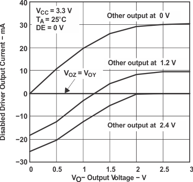 Figure 1. Disabled Driver Output Current vs Output Voltage
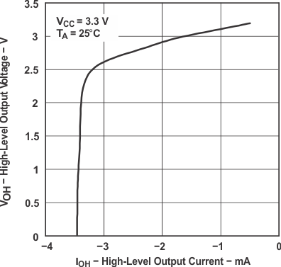 Figure 3. Driver High-Level Output Voltage vs High-Level Output Current
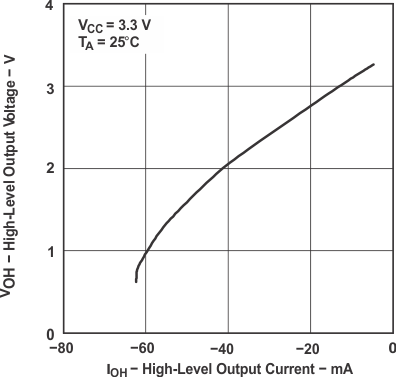 Figure 5. Receiver High-Level Output Voltage vs High-Level Output Current
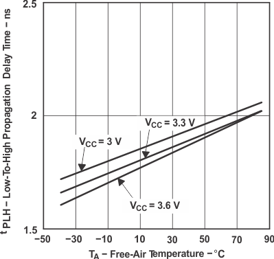 Figure 7. Driver Low-to-High Level Propagation Delay Time vs Free-Air Temperature
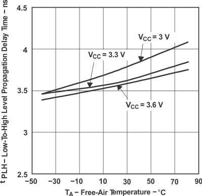 Figure 9. Receiver Low-to-High Level Propagation Delay Time vs Free-Air Temperature
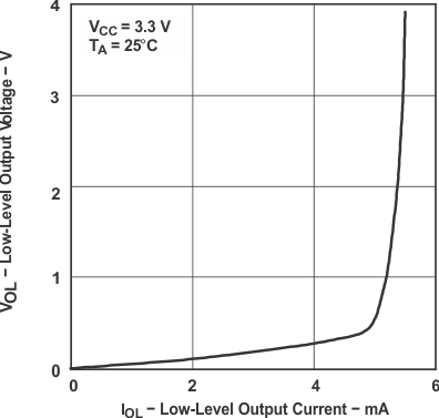 Figure 2. Driver Low-Level Output Voltage vs Low-Level Output Current
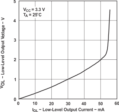 Figure 4. Receiver Low-Level Output Voltage vs Low-Level Output Current
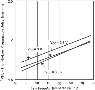 Figure 6. Driver High-to-Low Level Propagation Delay Time vs Free-Air Temperature
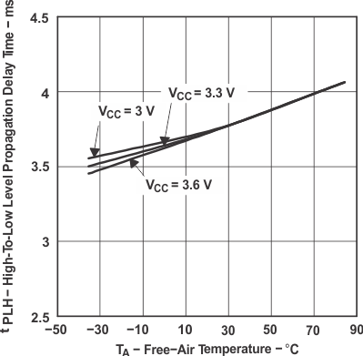 Figure 8. Receiver High-to-Low Level Propagation Delay Time vs Free-Air Temperature