SLLS301R APRIL 1998 – January 2016 SN65LVDS050 , SN65LVDS051 , SN65LVDS179 , SN65LVDS180
PRODUCTION DATA.
- 1 Features
- 2 Applications
- 3 Description
- 4 Revision History
- 5 Description (Continued)
- 6 Device Options
- 7 Pin Configuration and Functions
-
8 Specifications
- 8.1 Absolute Maximum Ratings
- 8.2 ESD Ratings
- 8.3 Recommended Operating Conditions
- 8.4 Thermal Information
- 8.5 Device Electrical Characteristics
- 8.6 Driver Electrical Characteristics
- 8.7 Receiver Electrical Characteristics
- 8.8 Driver Switching Characteristics
- 8.9 Receiver Switching Characteristics
- 8.10 Typical Characteristics
- 9 Parameter Measurement Information
- 10Detailed Description
- 11Application and Implementation
- 12Power Supply Recommendations
- 13Layout
- 14Device and Documentation Support
- 15Mechanical, Packaging, and Orderable Information
Package Options
Refer to the PDF data sheet for device specific package drawings
Mechanical Data (Package|Pins)
- PW|16
- D|16
Thermal pad, mechanical data (Package|Pins)
Orderable Information
9 Parameter Measurement Information
9.1 Driver
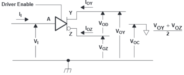 Figure 10. Driver Voltage and Current Definitions
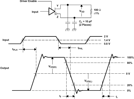
A. All input pulses are supplied by a generator having the following characteristics: tr or tf ≤ 1 ns, pulse repetition rate (PRR) = 50 Mpps, pulse width = 10 ± 0.2 ns. CL includes instrumentation and fixture capacitance within 0.06 mm of the device under test.
Figure 11. Test Circuit, Timing, and Voltage Definitions for the Differential Output Signal

A. All input pulses are supplied by a generator having the following characteristics: tr or tf ≤ 1 ns, pulse repetition rate (PRR) = 50 Mpps, pulse width = 10 ± 0.2 ns. CL includes instrumentation and fixture capacitance within 0.06 mm of the device under test. The measurement of VOC(PP) is made on test equipment with a –3-dB bandwidth of at least 300 MHz.
Figure 12. Test Circuit and Definitions for the Driver Common-Mode Output Voltage
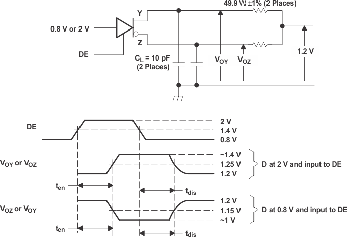
A. All input pulses are supplied by a generator having the following characteristics: tr or tf ≤ 1 ns, pulse repetition rate (PRR) = 0.5 Mpps, pulse width = 500 ± 10 ns. CL includes instrumentation and fixture capacitance within 0.06 mm of the device under test.
Figure 13. Enable or Disable Time Circuit and Definitions
9.2 Receiver
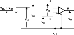 Figure 14. Receiver Voltage Definitions
Table 2. Receiver Minimum And Maximum Input Threshold Test Voltages
| APPLIED VOLTAGES | RESULTING DIFFERENTIAL INPUT VOLTAGE |
RESULTING COMMON-MODE INPUT VOLTAGE |
|
|---|---|---|---|
| VIA (V) | VIB (V) | VID (mV) | VIC (V) |
| 1.25 | 1.15 | 100 | 1.2 |
| 1.15 | 1.25 | –100 | 1.2 |
| 2.4 | 2.3 | 100 | 2.35 |
| 2.3 | 2.4 | –100 | 2.35 |
| 0.1 | 0 | 100 | 0.05 |
| 0 | 0.1 | –100 | 0.05 |
| 1.5 | 0.9 | 600 | 1.2 |
| 0.9 | 1.5 | –600 | 1.2 |
| 2.4 | 1.8 | 600 | 2.1 |
| 1.8 | 2.4 | –600 | 2.1 |
| 0.6 | 0 | 600 | 0.3 |
| 0 | 0.6 | –600 | 0.3 |
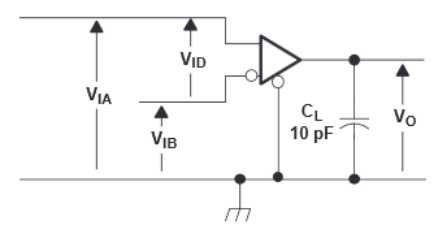
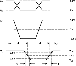
A. All input pulses are supplied by a generator having the following characteristics: tr or tf ≤ 1 ns, pulse repetition rate (PRR) = 50 Mpps, pulse width = 10 ± 0.2 ns. CL includes instrumentation and fixture capacitance within 0.06 m of the device under test.
Figure 15. Timing Test Circuit and Waveforms
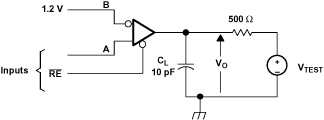
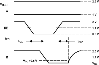
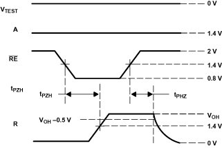
A. All input pulses are supplied by a generator having the following characteristics: tr or tf ≤ 1 ns, pulse repetition rate (PRR) = 0.5 Mpps, pulse width = 500 ± 10 ns. CL includes instrumentation and fixture capacitance within 0.06 m of the device under test.
Figure 16. Enable or Disable Time Test Circuit and Waveforms