SLLS881G December 2007 – October 2014 SN65LVDS315
PRODUCTION DATA.
- 1 Features
- 2 Applications
- 3 Description
- 4 Revision History
- 5 Pin Configuration and Functions
- 6 Specifications
- 7 Parameter Measurement Information
-
8 Detailed Description
- 8.1 Overview
- 8.2 Functional Block Diagram
- 8.3
Feature Description
- 8.3.1 Frame Counter Size
- 8.3.2 Data Formats
- 8.3.3 Parallel Input Port Timing Information
- 8.3.4 MIPI CSI-1 / CCP2-Class 0 Interface
- 8.3.5 Frame Structure and Synchronization Codes
- 8.3.6 Preventing Wrong Synchronization
- 8.3.7 Frame Structure
- 8.3.8 VS and HS Timing to Generate the Correct Control Signals
- 8.4 Device Functional Modes
- 9 Application and Implementation
- 10Power Supply Recommendations
- 11Layout
- 12Device and Documentation Support
- 13Mechanical, Packaging, and Orderable Information
Package Options
Mechanical Data (Package|Pins)
- RGE|24
Thermal pad, mechanical data (Package|Pins)
- RGE|24
Orderable Information
8 Detailed Description
8.1 Overview
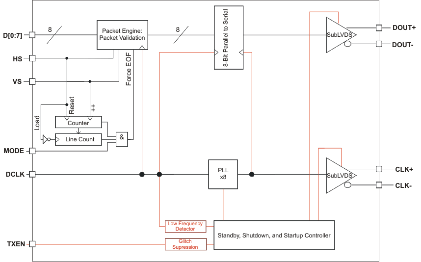
The SN65LVDS315 is a camera serializer that converts 8-bit parallel camera data into MIPI-CSI1 or SMIA CCP compliant serial signals.
The parallel data is latched in with the pixel clock input DCLK on the falling clock edge (D0 :D7), and the control inputs VS and HS are used to determine line and frame synchronization. According the state of HS and VS, the SN65LVDS315 shall generate a synchronization code (Start of frame SOF, End Of Frame EOF, Start Of Line SOL and End Of Line EOL) which will be included into the streaming data. Subsequently The latched data are serialized and transmitted by the SubLVDS driver (could be either input data or synchronization code). And the frequency of the differential output clock is eight times the input pixel clock rate.
The SN65LVDS315 has implemented an extra control for each frame size. If the MODE pin is high, then the device shall generate an EOF synchronization code when the number of transmitted lines belonging to the same frame reach the maximum allowed, in order to avoid a frame overflow.
The SN65LVDS315 supports three power modes (shutdown, standby and active) to conserve power. The TXEN input may be used to put the SN65LVDS315 in a shutdown mode. The SN65LVDS315 enters an active standby mode if the input clock, DCLK, stops. This minimizes power consumption without the need for controlling an external pin.
8.2 Functional Block Diagram
8.3 Feature Description
8.3.1 Frame Counter Size
The maximum size of frame_count is limited to 2046 lines. Transmitting more than 2046 active lines within one frame causes an error if MODE is held high.
8.3.2 Data Formats
The SN65LVDS315 supports the transfer of following data formats:
Table 4. Supported Data Formats
| DATA TYPE | ABBR. | COMMENT |
|---|---|---|
| YUV 422 image data | YUV422 | D[0:7] inputs are used as data inputs; The host processor must be configured to receive YUV 422 data; the SN65LVDS315 is transparent to these data formats (no special configuration required); The camera sensor must provide a UYVY output data sequence (e.g. U1,Y1,V1,Y2,U2,Y3,V3,Y4,U3,Y5...) |
| YUV 420 image data | YUV420 | D[0:7] inputs are used as data inputs; The host processor must be configured to receive YUV 420 data; the SN65LVDS315 is transparent to these data formats (no special configuration required); The camera sensor must provide an odd/even (or UYY.../ VYY...) output data sequence (e.g. odd like U1,Y1,Y2,U3,Y3,Y4,... followed by an even line V1,Y1,Y2,V3,Y3,Y4,...) |
| RGB 888 image data | RGB888 | D[0:7] inputs are used as data inputs; The host processor must be configured to receive RGB888 data; the SN65LVDS315 is transparent to these data formats (no special configuration required); The camera sensor must provide an output data sequence of B1,G1,R1,B2,G2,R2,... |
| RGB 565 image data | RGB565 | This data format can only be supported if the camera sensor outputs a 16-bit data format (two output bytes of 8-bit each) with the following format: |
| First byte: B[0:4] and G[0:2] (G2 is MSB on device input D7) | ||
| Second byte: G[3:5] and R[0:4] (R4 is MSB on device input D7) | ||
| Raw bayer, 8-bit image data | RAW8 | D[0:7] inputs are used as data inputs; The host processor must be configured to receive RAW8 data; The camera line length should be a multiple of 4 pixel; the SN65LVDS315 is transparent to these data formats (no special configuration required); The camera sensor must provide an output data sequence of P1,P2,P3,P4,,... |
Following data formats are not supported by the SN65LVDS315:
| – | RGB 444 image data | – | Raw Bayer 10-bit image data |
| – | Raw Bayer 6-bit image data | – | Raw Bayer 12-bit image data |
| – | Raw Bayer 7-bit image data | – | JPEG 8-bit data |
8.3.3 Parallel Input Port Timing Information
The parallel input data must comply with the following signal timing:
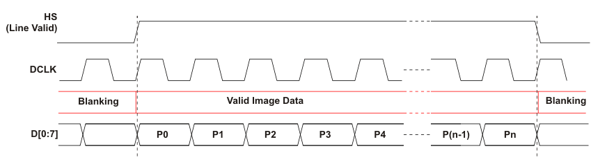 Figure 16. Parallel Input Timing Diagram
The relationship between frame sync and line sync shall be the following:
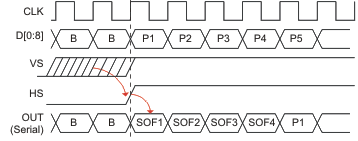
8.3.4 MIPI CSI-1 / CCP2-Class 0 Interface
When MODE is held low, the SN65LVDS315 provides a MIPI CSI-1 compliant serial output. The output data on DOUT is set on each falling edge of the differential clock signal, CLK. The CSI-1/CCP2 receiver should latch the data in on the rising CLK edge. The clock signal is free running (and not gated as optional in the CCP2 spec). The data format is bytewise (8-bit boundary) with the least significant bit (LSB) sent first. When nothing is being transferred (e.g. during blanking), DOUT remains high, except during power shutdown.
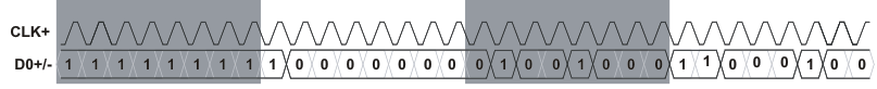 Figure 18. Data and Clock Output in CSI-1/CCP2
 Camera Mode Class-0 Transferring a Data Sequence of 0XFF011223H
8.3.5 Frame Structure and Synchronization Codes
Camera images are transferred in frames. Each frame contains one camera image. Each frame consists of a number of lines. A frame is always larger than the number of visible lines. The non-visible lines within a frame are called frame blanking. Frame blanking must be signaled on the SN65LVDS315 parallel input via a low VS signal. Each line within a frame has an invisible area as well — this area is called line blanking, and is indicated with a low HS signal. The CSI-1/CCP2-compliant output only transmits visible pixels within each frame. During line and frame blanking (also called horizontal and vertical blanking), the data output is set high. To indicate the line start, line end, frame start, and frame end, the SN65LVDS315 transmits synchronization codes.
Four synchronization codes are generated and embedded in the serial bit-stream:
| Start Of Line Code | SOL=0xFF00:0000 | This code identifies the start of a new line SOL; It is received for every line, except for the first line, which starts with a FSC |
| End Of Line Code | EOL=0xFF00:0001 | This code identifies the end of a line EOL; It is received for every line, except for the last line, which ends with a FEC |
| Start of Frame Code | SOF=0xFF00:0002 | This code identifies the start of a new frame SOF |
| End of Frame Code | EOF=0xFF00:0003 | This code identifies the end of the last line and the end of the current frame EOF |
Every synchronization code is transmitted byte-wise least significant bit (LSB) first. For example, the code 0xFF00:0002 transmitted from the image sensor corresponds to the following bit stream: 11111111 – 00000000 – 00000000 – 01000000.
Every default code starts with a set of eight 1s and sixteen 0s that are never received in pixel data (as having eight 1s and sixteen 0s is not allowed in pixel data).
8.3.6 Preventing Wrong Synchronization
To avoid actual pixel data from being erroneously interpreted as a control command, the SN65LVDS315 incorporates bit manipulation. If the SN65LVDS315 parallel input detects a bit sequence of eight 1s followed by sixteen 0s, it replaces the LSB of the 0x00 parallel input word with a one instead of a zero (so the actual pixel value will be adjusted from 0x00 to 0x01). Here are a few examples:
| input code on DIN: 0xFF.00.00 | serial output sequence on D0: 0xFF.00.01 |
| input code on DIN: 0xFE.01.00.00 | serial output sequence on D0: 0xFE.01.01.00 |
| D[7:0] parallel input Code | serial output code before correction | ||||||
|---|---|---|---|---|---|---|---|
| Byte 1 | Byte 2 | Byte 3 | Byte 4 | ||||
| MSB—LSB | MSB—LSB | MSB—LSB | MSB—LSB | ---time-------------------------------------------→ | |||
| 11111111 | 00000000 | 00000000 | xxxxxxxx | 11111111 | 00000000 | 00000000 | xxxxxxxx |
| 1111111x | 00000001 | 00000000 | xxxxxxx0 | x1111111 | 10000000 | 00000000 | 0xxxxxxx |
| 111111xx | 00000011 | 00000000 | xxxxxx00 | xx111111 | 11000000 | 00000000 | 00xxxxxx |
| 11111xxx | 00000111 | 00000000 | xxxxx000 | xxx11111 | 11100000 | 00000000 | 000xxxxx |
| 1111xxxx | 00001111 | 00000000 | xxxx0000 | xxxx1111 | 11110000 | 00000000 | 0000xxxx |
| 111xxxxx | 00011111 | 00000000 | xxx00000 | xxxxx111 | 11111000 | 00000000 | 00000xxx |
| 11xxxxxx | 00111111 | 00000000 | xx000000 | xxxxxx11 | 11111100 | 00000000 | 000000xx |
| 1xxxxxxx | 01111111 | 00000000 | x0000000 | xxxxxxx1 | 11111110 | 00000000 | 0000000x |
| ↓ ↓ | ↓ ↓ | ||||||
| D[7:0] parallel input Code (corrected) | serial output code after correction | ||||||
| Byte 1 | Byte 2 | Byte 3 | Byte 4 | ||||
| MSB—LSB | MSB—LSB | MSB—LSB | MSB—LSB | ---time------------------------------------------------------→ | |||
| 11111111 | 00000000 | 00000001 | xxxxxxxx | 11111111 | 00000000 | 10000000 | xxxxxxxx |
| 1111111x | 00000001 | 00000001 | xxxxxxx0 | x1111111 | 10000000 | 10000000 | 0xxxxxxx |
| 111111xx | 00000011 | 00000001 | xxxxxx00 | xx111111 | 11000000 | 10000000 | 00xxxxxx |
| 11111xxx | 00000111 | 00000001 | xxxxx000 | xxx11111 | 11100000 | 10000000 | 000xxxxx |
| 1111xxxx | 00001111 | 00000001 | xxxx0000 | xxxx1111 | 11110000 | 10000000 | 0000xxxx |
| 111xxxxx | 00011111 | 00000001 | xxx00000 | xxxxx111 | 11111000 | 10000000 | 00000xxx |
| 11xxxxxx | 00111111 | 00000001 | xx000000 | xxxxxx11 | 11111100 | 10000000 | 000000xx |
| 1xxxxxxx | 01111111 | 00000001 | x0000000 | xxxxxxx1 | 11111110 | 10000000 | 0000000x |
8.3.7 Frame Structure
The next two graphs show the construction and transmission of a frame:
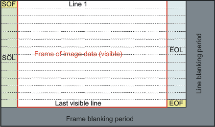 Figure 19. Frame Structure
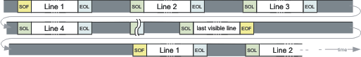 Figure 20. Data and Clock Output in CSI-1 / CCP2 Camera Mode Class-0 Transferring a Data Sequence of 0XFF011223H
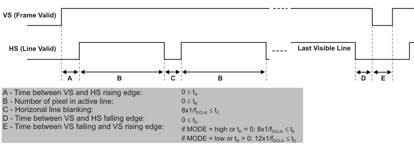
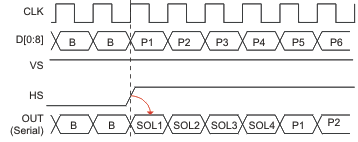
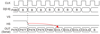
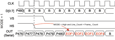
8.3.8 VS and HS Timing to Generate the Correct Control Signals
The VS and HS timing received from camera sensors varies. The SN65LVDS315 responds in the following way:
|
Frame Start and Line Start
|
 |
|
Any additional rising edge on HS initiates transmission of SOL until VS is de-asserted to low. |
 |
|
Line End and Frame End
|
 |
|
If HS and VS are set low with the same DCLK cycle, the device will transmit EOF instead of EOL. |
 |
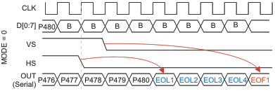
Ideally, the VS and HS falling edge occur during the same clock period. In such case, the MODE input can be kept low (MODE=0), and the response of the SN65LVDS315 output to the parallel input data looks like the following:
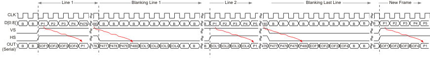 Figure 21. VS and HS Timing
Caution: Some camera sensors generate a frame sync (VS) signal that lasts longer than the HS of the last visible line. In such case, and with MODE = low, the SN65LVDS315 transmits EOL during the last HS low transition and transmits EOF when VS transitions low. If the CSI-1 receiver can tolerate receiving EOL followed by EOF, it is recommended to keep the MODE input pin set to low.
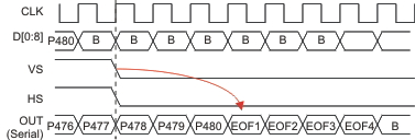
If the CSI-1 receiver cannot tolerate reception of an EOL packet followed by an EOF packet, the SN65LVDS315 can also be configured in a mode that allows it to predict the number of visible lines and generate an EOF packet at the proper time. A high level on the the MODE input enables a line counter within the SN65LVDS315 that counts every HS rising edge while VS is high. The OMAP processors require the MODE signal to be set high.
The counter value is stored into register frame_count when VS transitions low and the counter is reset to zero. When the counter reaches the value stored in frame_count, an EOF packet is transmitted instead of the EOL packet. As long as the active number of lines remains constant, this implementation ensures proper transmission of EOF.
If, however, the camera sensor changes the number of transmitted lines during active transmission, the EOF will not be generated properly for that particular frame.
If the number of lines transmitted by the camera sensor increases, an EOF will be sent too early. All active lines following EOF are then ignored during this particular frame. Blanking will be signaled instead. The frame_count register will be updated at the end of the frame in order to properly transmit the next frame.
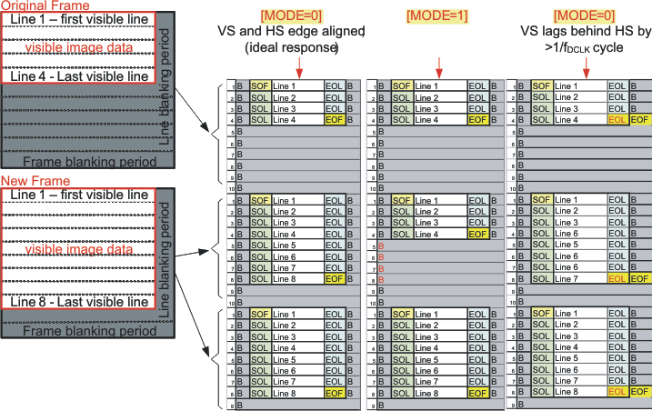 Figure 22. MODE Implementation Example 1
If the number of lines transmitted by the camera sensor decreases, EOL will be sent improperly after the last camera line. When VS is detected low, the EOF command will follow.
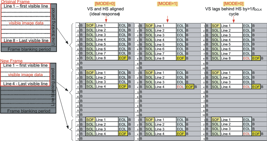 Figure 23. MODE Implementation Example 2
8.4 Device Functional Modes
8.4.1 Powerdown Modes
The SN65LVDS315 transmitter has two power-down modes to facilitate efficient power management.
8.4.1.1 Shutdown Mode
The SN65LVDS315 enters shutdown mode when the TXEN terminal is asserted low. This turns off all transmitter circuitry, including the CMOS input, PLL, serializer, and SubLVDS transmitter output stage. All outputs are high impedance. Current consumption in shutdown mode is nearly zero.
8.4.1.2 Standby Mode
The SN65LVDS315 enters the standby mode if TXEN is high and the DCLK input signal frequency is less than 500 kHz. All circuitry except the DCLK input monitor is shut down, and all outputs enter the high-impedance state. The current consumption in standby mode is low. When the DCLK input signal is completely stopped, the IDD current consumption is minimized.
NOTE
Leaving the TXEN, FSEL or MODE input floating (left open) allows leakage currents to flow from VDD to GND. To prevent excessive leakage current, a CMOS gate must be kept at a valid logic level, either high (above VIH min) or low (below VIL min). This can be achieved by applying an external voltage or ground to these inputs. Inputs Dx, VS, HS, and DCLK incorporate bus hold, and can be left floating or tied high or low. Switching inputs also causes increased leakage currents. Only if no input signal is switching will the IDD current be at its minimum.
8.4.2 Active Modes
When TXEN is high and the DCLK input clock frequency is higher than 3 MHz, the SN65LVDS315 enters the active mode. Current consumption in the active mode depends on operating frequency and the number of data transitions in the data payload.
8.4.2.1 Acquire Mode (PLL Approaches Lock)
The PLL is enabled and attempts to lock to the input clock. All outputs remain in the high-impedance state. First, the PLL monitor waits until it detects stable PLL operation. If MODE is set low, the digital core will wait for one VS low-to-high transition (new frame start) before the device switches from the acquire mode to the transmit mode. This ensures that the outputs turn on when a new image frame is transmitted by the camera sensor. If MODE is set high, the digital core will wait for two (instead of one) VS low-to-high transitions before the device switches from the acquire mode to the transmit mode. This not only ensures that the device waits for a new camera frame, but also allows the internal SN65LVDS315 counter to be initiated with the proper line count. For proper device operation, the pixel-clock frequency (fDCLK) must fall within the valid fDCLK range specified under recommended operating conditions. If the pixel clock frequency is higher than 3 MHz but lower than fDCLK(min), the SN65LVDS315 PLL is enabled. Under such conditions, it is possible for the PLL to lock temporarily to the pixel clock, causing the PLL monitor to release the device into transmit mode. If this happens, the PLL may or may not be properly locked to the pixel clock input, potentially causing data errors, frequency oscillation, and PLL deadlock (loss of VCO oscillation).
8.4.2.2 Transmit Mode
After the PLL achieves lock, the device enters the normal transmit mode. The CLK and DOUT terminals output CSI-1 compliant serial data.
8.4.3 Status Detect and Operating Modes Flow Diagram
The SN65LVDS315 switches between the power saving and active modes in the following way:
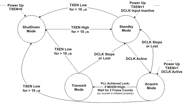 Figure 24. Status Detect and Operating Modes Flow Diagram
Table 5. Status Detect and Operating Modes Descriptions
| MODE | CHARACTERISTICS | CONDITIONS |
|---|---|---|
| Shutdown Mode | Least amount of power consumption (most circuitry turned off); All outputs high impedance. | TXEN is low for longer than 10 μs(1)(2) |
| Standby Mode | Low power consumption (only clock activity circuit active; PLL is disabled to conserve power); all outputs are high impedance. | TXEN is high for longer than 10 μs; DCLK input signal is missing or inactive. (2) |
| Acquire Mode | PLL tries to achieve lock; if MODE is high, initiate line counter (to place EOF at proper position); All outputs are high impedance. | TXEN is high; DCLK input monitor detected input activity. |
| Transmit Mode | Data transfer (normal operation); transmitter serializes data and transmits data on serial output. | TXEN is high and PLL is locked to the incoming clock. |
Table 6. Mode Transition Use Cases
| MODE TRANSITION | USE CASE | TRANSITION SPECIFICS | |
|---|---|---|---|
| Shutdown -> Standby | Set TXEN high to enable transmitter | 1. | TXEN high > 10 μs |
| 2. | Transmitter enters Standby mode | ||
| a. All outputs are in high-impedance state. | |||
| b. Transmitter turns on clock input monitor | |||
| Standby-> Acquire | DCLK input activity detected | 1. | DCLK input monitor detects clock input activity; |
| 2. | Outputs remain in high-impedance state. | ||
| 3. | PLL circuit is enabled | ||
| Acquire -> Transmit | Device is ready to transfer data | 1. | PLL is active and approaches lock |
| 2. | PLL achieves lock within twakeup | ||
| 3. | Parallel data input latches into shift register. | ||
| 4. | Data input patterns are monitored and the line counter is initialized | ||
| 5. | CLK output turns on | ||
| 6. | DOUT turns on and sends out first serial data bit. | ||
| Transmit -> Standby | Request transmitter to enter standby mode by stopping DCLK | 1. | DCLK Input monitor detects missing DCLK. |
| 2. | Transmitter indicates standby, putting all outputs into high-impedance state. | ||
| 3. | PLL shuts down. | ||
| 4. | DCLK activity input monitor remains active. | ||
| Transmit/Standby -> Shutdown | Turn off transmitter by pulling TXEN low | 1. | TXEN pulled low for > tpwrdn. |
| 2. | Transmitter indicates standby by switching output CLK+ and CLK– into high-impedance state. | ||
| 3. | Transmitter drives DOUT into high-impedance state. | ||
| 4. | Most IC circuitry is shut down for least power consumption. | ||