SLLS881G December 2007 – October 2014 SN65LVDS315
PRODUCTION DATA.
- 1 Features
- 2 Applications
- 3 Description
- 4 Revision History
- 5 Pin Configuration and Functions
- 6 Specifications
- 7 Parameter Measurement Information
-
8 Detailed Description
- 8.1 Overview
- 8.2 Functional Block Diagram
- 8.3
Feature Description
- 8.3.1 Frame Counter Size
- 8.3.2 Data Formats
- 8.3.3 Parallel Input Port Timing Information
- 8.3.4 MIPI CSI-1 / CCP2-Class 0 Interface
- 8.3.5 Frame Structure and Synchronization Codes
- 8.3.6 Preventing Wrong Synchronization
- 8.3.7 Frame Structure
- 8.3.8 VS and HS Timing to Generate the Correct Control Signals
- 8.4 Device Functional Modes
- 9 Application and Implementation
- 10Power Supply Recommendations
- 11Layout
- 12Device and Documentation Support
- 13Mechanical, Packaging, and Orderable Information
Package Options
Mechanical Data (Package|Pins)
- RGE|24
Thermal pad, mechanical data (Package|Pins)
- RGE|24
Orderable Information
6 Specifications
6.1 Absolute Maximum Ratings(1)
| MIN | MAX | UNIT | ||
|---|---|---|---|---|
| Supply voltage range(2) | VDDIO | –0.3 | 4 | V |
| VDDD, VDDA | –0.3 | 2.175 | V | |
| Voltage range at any output terminal | –0.5 | 2.175 | V | |
| Voltage range at any input terminal | –0.5 | VDDIO + 0.5 | V | |
| Continuous power dissipation | See Thermal Information | |||
(1) Stresses beyond those listed under Absolute Maximum Ratings may cause permanent damage to the device. These are stress ratings only and functional operation of the device at these or any other conditions beyond those indicated under Recommended Operating Conditions is not implied. Exposure to absolute maximum- rated conditions for extended periods may affect device reliability.
(2) All voltage values are with respect to the GND pins.
6.2 Handling Ratings
| MIN | MAX | UNIT | |||
|---|---|---|---|---|---|
| Tstg | Storage temperature range | –65 | 150 | °C | |
| V(ESD) | Electrostatic discharge | Human body model(1) (All pins) | –3 | 3 | kV |
| Charged device model(2) (All pins) | –500 | 500 | V | ||
| Machine model(3) (All pins) | –200 | 200 | |||
(1) In accordance with JEDEC Standard 22, Test Method A114-A.
(2) In accordance with JEDEC Standard 22, Test Method C101.
(3) In accordance with JEDEC Standard 22, Test Method A115-A
6.3 Recommended Operating Conditions
Unused single-ended inputs must be held high or low to prevent them from floating.| MIN | NOM | MAX | UNIT | |||
|---|---|---|---|---|---|---|
| VDDIO
VDDD VDDA |
Supply voltage | 1.65 1.65 1.65 |
1.8 1.8 |
3.6 1.95 1.95 |
V | |
| VDDn(PP) | Supply voltage noise magnitude | f(VDDn(PP)) = 1 Hz to 2 GHz (test set-up see Figure 13) | 100 | mV | ||
| fDCLK | Data clock frequency | FSEL = 0, See Figure 16, Figure 17, Figure 18 | 3.5 | 13 | MHz | |
| FSEL = 1, See Figure 16, Figure 17, Figure 18 | 7 | 27 | ||||
| Standby mode (1) | 500 | kHz | ||||
| tH x fDCLK | DCLK Input duty cycle | 0.35 | 0.65 | |||
| TA | Operating free-air temperature | –40 | 85 | °C | ||
| tjit(per)DCLK | DCLK RMS period jitter(2) | Measured on DCLK input | 5 | ps-rms | ||
| tjit(TJ)DCLK | DCLK total jitter(3) | 0.05/fDCLK | s | |||
| tjit(CC)DCLK | DCLK peak cycle to cycle jitter(4) | 0.02/fDCLK | s | |||
| Icount | Number of active video lines(5) | MODE = VIH; count the number of HS↓ transitions within one frame | 1 | 2046 | ||
| thblank | Horizontal blanking time | 4 | UI (1/DCLK) |
|||
| tvblank | Vertical blanking time | 8 | UI (1/DCLK) |
|||
| DCLK, D[0:1], VS, HS | ||||||
| VIH | High-level input voltage | See Figure 7 | 0.7×VDDIO | VDDIO | V | |
| VIL | Low-level input voltage | See Figure 7 | 0 | 0.3×VDDIO | V | |
| tDS | Data set up time prior to ↑↓ DCLK | See Figure 8 | 2.0 | ns | ||
| tDH | Data hold time after ↑↓ DCLK | See Figure 8 | 2.0 | ns | ||
| MODE, TXEN | ||||||
| VIH | High-level input voltage | See Figure 7 | 0.7×VDDA | 3.6 | V | |
| VIL | Low-level input voltage | See Figure 7 | 0 | 0.3×VDDA | V | |
| FSEL | ||||||
| VIH | High-level input voltage | See Figure 7 | 0.7×VDDD | 3.6 | V | |
| VIL | Low-level input voltage | See Figure 7 | 0 | 0.3×VDDD | V | |
(1) DCLK input frequencies lower than 500 kHz will force the SN65LVDS315 into standby mode. Input frequencies between 500 kHz and 3 MHz might activate the SN65LVDS315. Input frequencies beyond 3MHz will activate the SN65LVDS315.
(2) Period jitter is the deviation in cycle time of a signal with respect to the ideal period over a random sample of 100,000 cycles.
(3) Total jitter reflects the maximum jitter amplitude observed over a time period of 1012 data bits. It is often derived by adding all deterministic jitter components (ps peak-to-peak values) and the geometric sum of all random components (ps-rms values × 14.069 for 10–12 bit error rate)
(4) Cycle-to-cycle jitter is the variation in cycle time of a signal between adjacent cycles over a random sample of 1,000 adjacent cycle pairs.
(5) For a VGA resolution of 640x480, lcount would be 480
6.4 Thermal Information
| THERMAL METRIC(1) | SN65LVDS315 | UNIT | |
|---|---|---|---|
| RGE | |||
| 24 PINS | |||
| RθJA | Junction-to-ambient thermal resistance | 38.2 | °C/W |
| RθJC(top) | Junction-to-case (top) thermal resistance | 41.3 | |
| RθJB | Junction-to-board thermal resistance | 16.1 | |
| ψJT | Junction-to-top characterization parameter | 0.9 | |
| ψJB | Junction-to-board characterization parameter | 16.1 | |
| RθJC(bot) | Junction-to-case (bottom) thermal resistance | 6.6 | |
(1) For more information about traditional and new thermal metrics, see the IC Package Thermal Metrics application report, SPRA953.
6.5 Device Electrical Characteristics
over operating free-air temperature range (unless otherwise noted)| PARAMETER | TEST CONDITIONS | MIN | TYP(1) | MAX | UNIT | ||
|---|---|---|---|---|---|---|---|
| IDD | Supply current | VDDIO = VDDD = VDDA, RL(CLK) = RL(D0) = 100 Ω, VIH=VDDIO, VIL=0V, TXEN and MODE at VDDD, typical blanking power test pattern. See Table 1 | FSEL = VIL, fDCLK = 3.5 MHz FSEL = VIL, fDCLK = 11 MHz FSEL = VIH, fDCLK = 11 MHz FSEL = VIH, fDCLK = 26 MHz |
4.8 7.6 5.9 9.6 |
mA | ||
| VDDIO = VDDD = VDDA, RL(CLK) = RL(D0) = 100 Ω, VIH=VDDIO, VIL=0V, TXEN and MODE at VDDD, Alternating (worst-case) 1010 serial bit pattern. See Table 2 | FSEL = VIL, fDCLK = 3.5 MHz FSEL = VIL, fDCLK = 11 MHz FSEL = VIH, fDCLK = 11 MHz FSEL = VIH, fDCLK = 26 MHz |
5.7 8.9 7.2 11.3 |
8.1 11.2 9.5 13.3 |
||||
| Standby mode (TXEN at VDD) | VDDIO = VDDD = VDDA, RL(CLK) = RL(D0) = 100 Ω, VIH=VDDIO, VIL=0 V, TXEN and MODE at VDDD, All inputs held static high (VIH) or static low (VIL) |
0.2 | 10 | μA | |||
| Shutdown mode (TXEN at GND) | 0.2 | 10 | |||||
| Standby mode (TXEN at VDD) | VDDIO = VDDD = VDDA, RL(CLK) = RL(D0) = 100 Ω, VIH=VDDIO, VIL=0 V, TXEN and Mode = VIL; D[7:0] VS, HS, and DCLK left open |
0.02 | 10 | ||||
| Shutdown mode (TXEN at GND) | 0.03 | 5 | |||||
| PD | Device power dissipation | VDDx = 1.8 V, TA = 25°C | fDCLK = 3.5 MHz fDCLK = 11 MHz fDCLK = 26 MHz |
10.8 17.7 21.2 |
mW | ||
| VDDx = 1.95 V, TA = –40°C | fDCLK = 3.5 MHz fDCLK = 26 MHz |
15.7 26.0 |
|||||
(1) All typical values are at 25°C and with 1.8 V supply unless otherwise noted.
6.6 Output Electrical Characteristics
over recommended operating conditions (unless otherwise noted)| PARAMETER | TEST CONDITIONS | MIN | TYP(1) | MAX | UNIT | |
|---|---|---|---|---|---|---|
| subLVDS OUTPUTS (DOUT+, DOUT–, CLK+, and CLK–) | ||||||
| VOCM(SS) | Steady-state common-mode output voltage | See Figure 7, Output load see Figure 11 | 0.8 | 0.925 | 1.0 | V |
| |VOD| | Differential output voltage magnitude |VDOUT+ – VDOUT– |, |VCLK+ – VCLK–| |
100 | 170 | 250 | mV | |
| Δ|VOD| | Change in differential output voltage between logic states | –10 | 10 | mV | ||
| ZOD | Differential small-signal output impedance | TXEN at VDD | 5 | kΩ | ||
| IOSD | Differential short-circuit output current | VOD = 0 V; fDCLK = 26 MHz | 1 | 10 | mA | |
| IOZ | High-impedance state output current | VO = 0 V or VDD(max), TXEN at GND | –3 | 3 | μA | |
(1) All typical values are at 25°C and with 1.8V supply unless otherwise noted.
6.7 Input Electrical Characteristics
over recommended operating conditions (unless otherwise noted)| PARAMETER | TEST CONDITIONS | MIN | TYP(1) | MAX | UNIT | |
|---|---|---|---|---|---|---|
| Dx, VS, HS, DCLK | ||||||
| IIL(hold) | Bus hold input current(2) | VDDIO = 1.65 V and VDDIO = 3.6 V | 15 | 100 | μA | |
| IIH(hold) | Bus hold input current(3) | VDDIO = 1.65 V and VDDIO = 3.6 V | –15 | –100 | μA | |
| CIN | Input capacitance | 1.5 | pF | |||
| MODE, TXEN, FSEL | ||||||
| IIL | High-level input current | VIH = 0.7 VDDD, See Figure 7 | –200 | –0.7 | 200 | nA |
| IIH | Low-level input current | VIL = 0.3 VDDD, See Figure 7 | –200 | 0.5 | 200 | nA |
| CIN | Input capacitance | VI = TBD | 1.5 | pF | ||
(1) All typical values are at 25°C and with 1.8 V supply unless otherwise noted.
(2) IIL(hold) is the input current the bus-hold input stage is able to source to maintain a low logic level; The bus-hold current becomes minimal as the input approaches GND. IIL(hold) is the least amount of current a camera output must source to overcome the bus hold and force a high signal.
(3) IIH(hold) is the input current the bus-hold input stage is able to source to maintain a high logic level. The bus-hold current becomes minimal as the input approaches VDDIO. IIL(hold) is the least amount of current a camera output must be able source to overcome the bus hold and switch to a low signal.
6.8 Switching Characteristics
over recommended operating conditions (unless otherwise noted)| PARAMETER | TEST CONDITIONS | MIN | TYP(1) | MAX | UNIT | ||
|---|---|---|---|---|---|---|---|
| tr | 20%-to-80% differential output signal rise time | fDCLK=3.5 MHz, See Figure 10 and Figure 11 | 360 | 460 | 730 | ps | |
| tf | 20%-to-80% differential output signal fall time | fDCLK=3.5 MHz, See Figure 10 and Figure 11 | 360 | 460 | 730 | ps | |
| ts(DOUT) | Setup time DOUT valid before CLK+ rising edge | See Figure 9 | FSEL = 0, fDCLK = 13 MHz FSEL = 1, fDCLK = 26 MHz |
3.327 1.163 |
4.2 1.8 |
ns | |
| th(DOUT) | Hold time DOUT valid before CLK+ ringing edge | FSEL = 0, fDCLK = 13 MHz FSEL = 1, fDCLK = 26 MHz |
4.627 2.463 |
5.4 3.0 |
ns | ||
| tpd(L) | Propagation delay time, input to serial output (data latency) | TXEN at VDDD, VIH = VDDD, VIL=GND, RL = 100 Ω, See Figure 12 |
4.5/fDCLK | 4.7/fDCLK | 5.5/fDCLK | ||
| tH x fCLKO | Output CLK duty cycle | 0.45 | 0.50 | 0.55 | |||
| tGS | TXEN glitch suppression pulse width(2) | VIH = VDDD, VIL=GND, TXEN toggles between VIL and VIH, See Figure 14 | 3.8 | 10 | μs | ||
| tpwnup | Enable time from power down (↑TXEN) | MODE at VDD; time from TXEDN pulled high to CLK and DOUT outputs enabled and transmit valid data; See Figure 14 | 100 | 100μs + 2×VS↑ | μs | ||
| tpwrdn | Disable time from active mode (↓TXEN) | TXEN is pulled low during transmit mode; time measurement until output becomes disabled and PLL is shutdown; See Figure 14 | 11 | μs | |||
| twakup | Enable time from standby (↑↓DCLK) | TXEN and MODE at VDD; device in standby; time measurement from DCLK starts switching to CLK and DOUT enabled and transmit valid data; See Figure 15 | 100 | 100μs + 2×VS↑ | μs | ||
| tsleep | Disable time from standby (DCLK stopping) | TXEN at VDD; device in transmitting; time measurement from DCLK input signal stops starts until CLK + DOUT outputs becomes disabled and PLL is shutdown, See Figure 15 | <8/fDCLK | 100 | μs | ||
(1) All typical values are at 25°C and with 1.8 V supply unless otherwise noted.
(2) The TXEN input incorporates glitch-suppression circuitry to disregard short input pulses. tGS is the duration of either a high-to-low or low-to-high transition that is suppressed.
6.9 Typical Characteristics
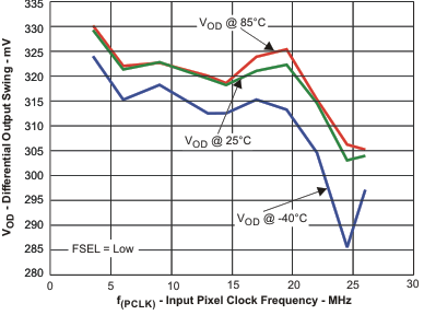
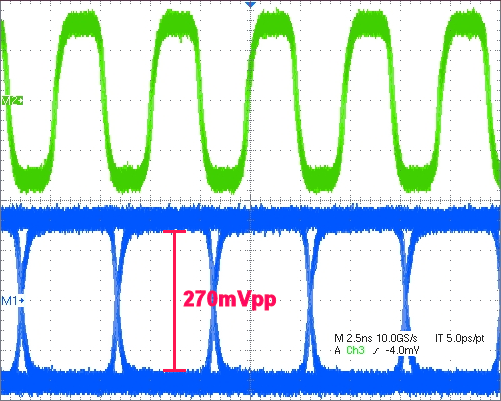
| FSEL = Low |
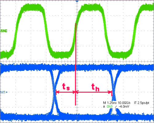
The asymmetrical setup and hold time is optimized to meet OMAP processor input timing.
Figure 5. SN65LVDS315 Output Data and Clock Signal at 208 mbps
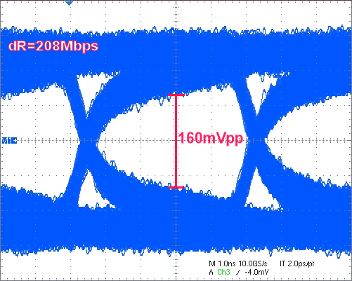
| Through pcb interconnect of 80-inch of FR4 at 208Mbps |