SLLS881G December 2007 – October 2014 SN65LVDS315
PRODUCTION DATA.
- 1 Features
- 2 Applications
- 3 Description
- 4 Revision History
- 5 Pin Configuration and Functions
- 6 Specifications
- 7 Parameter Measurement Information
-
8 Detailed Description
- 8.1 Overview
- 8.2 Functional Block Diagram
- 8.3
Feature Description
- 8.3.1 Frame Counter Size
- 8.3.2 Data Formats
- 8.3.3 Parallel Input Port Timing Information
- 8.3.4 MIPI CSI-1 / CCP2-Class 0 Interface
- 8.3.5 Frame Structure and Synchronization Codes
- 8.3.6 Preventing Wrong Synchronization
- 8.3.7 Frame Structure
- 8.3.8 VS and HS Timing to Generate the Correct Control Signals
- 8.4 Device Functional Modes
- 9 Application and Implementation
- 10Power Supply Recommendations
- 11Layout
- 12Device and Documentation Support
- 13Mechanical, Packaging, and Orderable Information
Package Options
Mechanical Data (Package|Pins)
- RGE|24
Thermal pad, mechanical data (Package|Pins)
- RGE|24
Orderable Information
7 Parameter Measurement Information
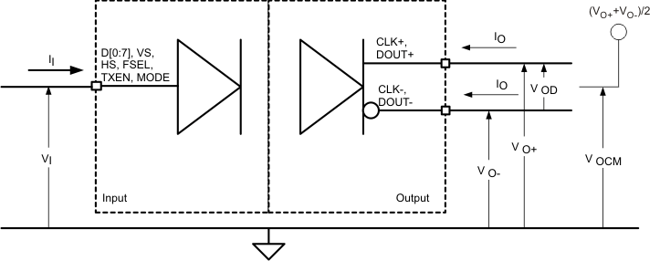 Figure 7. I/O Voltage and Current Definition
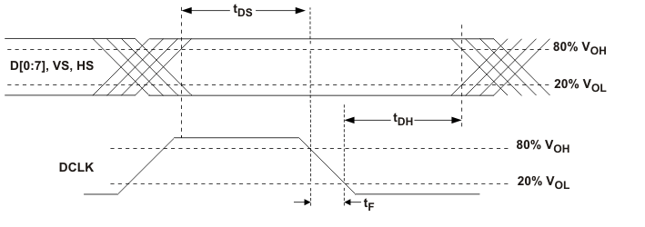 Figure 8. Input Signal Setup and Hold Time Definition TDS And TDH
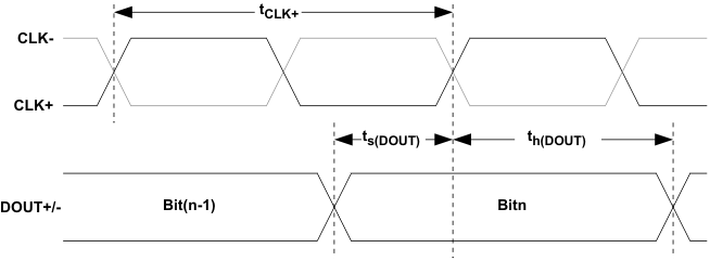 Figure 9. Output Signal Setup and Hold Time Definition Ts(DOUT) And Th(DOUT)
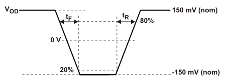 Figure 10. Rise and Fall Time Definition
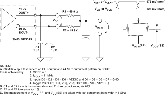 Figure 11. Driver Output Voltage Test Circuit and Definitions
 Figure 12. TPD(L) Propagation Delay Input to Output
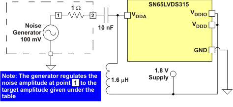 Figure 13. Power Supply Noise Test Set-Up
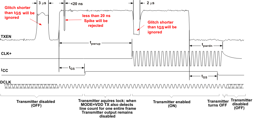 Figure 14. Glitch Suppression Enable/Disable Time
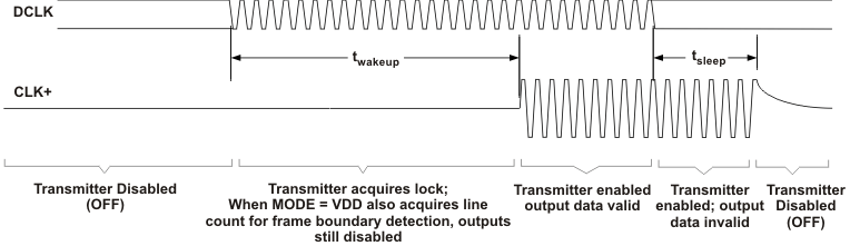 Figure 15. Standby Detection
7.1 Typical Blanking Power Consumption Test Pattern
During blanking VS is low, and the SN65LVDS315 data output DOUT presents a high signal. The typical power consumption test patterns during the blanking time consists of one data word. The pattern repeats itself throughout the entire measurement.
Table 1. Typical IC Power Consumption Test During Blanking
| WORD | TEST PATTERN | ||
|---|---|---|---|
| D[7:0] | VS | HS | |
| 1 | 0x00 | 0 | x |
7.2 Maximum Power Consumption Test Pattern
The maximum (or worst-case) power consumption of the SN65LVDS315 is tested using an alternating 1010 test pattern. The pattern repeats itself throughout the entire measurement.
Table 2. Worst Case IC Power Consumption Test Pattern 1
| WORD | TEST PATTERN | ||
|---|---|---|---|
| D[7:0] | VS | HS | |
| 1 | 0x00 | 1 | 1 |
| 2 | 0xFF | 1 | 1 |
7.3 Jitter Performance
The jitter performance of the SN65LVDS315 is tested using a pattern that stresses the interconnect, particularly to test for ISI. The test pattern uses very long run lengths of consecutive bits. The pattern incorporates very high and low data rates, and maximizes switching noise. The pattern is self-repeating for the duration of the test.
Table 3. Jitter Test Pattern
| WORD | TEST PATTERN | ||
|---|---|---|---|
| D[7:0] | VS | HS | |
| 1 | 0x00 | 1 | 1 |
| 2 | 0x00 | 1 | 1 |
| 3 | 0x00 | 1 | 1 |
| 4 | 0x01 | 1 | 1 |
| 5 | 0x03 | 1 | 1 |
| 6 | 0x07 | 1 | 1 |
| 7 | 0x18 | 1 | 1 |
| 8 | 0xE7 | 1 | 1 |
| 9 | 0x35 | 1 | 1 |
| 10 | 0x02 | 1 | 1 |
| 11 | 0x54 | 1 | 1 |
| 12 | 0xA5 | 1 | 1 |
| 13 | 0xAD | 1 | 1 |
| 14 | 0x55 | 1 | 1 |
| 15 | 0xA6 | 1 | 1 |
| 16 | 0xA6 | 1 | 1 |
| 17 | 0x55 | 1 | 1 |
| 18 | 0x55 | 1 | 1 |
| 19 | 0xAA | 1 | 1 |
| 20 | 0x52 | 1 | 1 |
| 21 | 0x5A | 1 | 1 |
| 22 | 0xAB | 1 | 1 |
| 23 | 0xFD | 1 | 1 |
| 24 | 0xCA | 1 | 1 |
| 25 | 0x18 | 1 | 1 |
| 26 | 0xE7 | 1 | 1 |
| 27 | 0xF8 | 1 | 1 |
| 28 | 0xFC | 1 | 1 |
| 29 | 0xFE | 1 | 1 |
| 30 | 0xFF | 1 | 1 |
| 31 | 0xFF | 1 | 1 |
| 32 | 0xFF | 1 | 1 |