SLLS881G December 2007 – October 2014 SN65LVDS315
PRODUCTION DATA.
- 1 Features
- 2 Applications
- 3 Description
- 4 Revision History
- 5 Pin Configuration and Functions
- 6 Specifications
- 7 Parameter Measurement Information
-
8 Detailed Description
- 8.1 Overview
- 8.2 Functional Block Diagram
- 8.3
Feature Description
- 8.3.1 Frame Counter Size
- 8.3.2 Data Formats
- 8.3.3 Parallel Input Port Timing Information
- 8.3.4 MIPI CSI-1 / CCP2-Class 0 Interface
- 8.3.5 Frame Structure and Synchronization Codes
- 8.3.6 Preventing Wrong Synchronization
- 8.3.7 Frame Structure
- 8.3.8 VS and HS Timing to Generate the Correct Control Signals
- 8.4 Device Functional Modes
- 9 Application and Implementation
- 10Power Supply Recommendations
- 11Layout
- 12Device and Documentation Support
- 13Mechanical, Packaging, and Orderable Information
Package Options
Mechanical Data (Package|Pins)
- RGE|24
Thermal pad, mechanical data (Package|Pins)
- RGE|24
Orderable Information
11 Layout
11.1 Layout Guidelines
- Use 45 degree bends (chamfered corners), instead of right-angle (90°) bends. Right-angle bends increase the effective trace width, which changes the differential trace impedance creating large discontinuities. A 45° bends is seen as a smaller discontinuity.
- Place passive components within the signal path, such as source-matching resistors or ac-coupling capacitors, next to each other. Routing as in case a) creates wider trace spacing than in b), the resulting discontinuity, however, is limited to a far narrower area.
- When routing traces next to a via or between an array of vias, make sure that the via clearance section does not interrupt the path of the return current on the ground plane below.
- Avoid metal layers and traces underneath or between the pads off the DisplayPort connectors for better impedance matching. Otherwise they will cause the differential impedance to drop below 75 Ω and fail the board during TDR testing.
- Use solid power and ground planes for 100 Ω impedance control and minimum power noise.
- For a multilayer PCB, it is recommended to keep one common GND layer underneath the device and connect all ground terminals directly to this plane.
- For 100 Ω differential impedance, use the smallest trace spacing possible, which is usually specified by the PCB vendor.
- Keep the trace length as short as possible to minimize attenuation.
- Place bulk capacitors (for example, 10 μF) close to power sources, such as voltage regulators or where the power is supplied to the PCB.
11.2 Layout Example
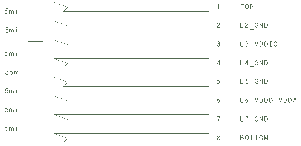 Figure 31. 8-Layers PCB Example
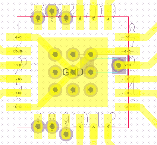 Figure 32. Footprint Example
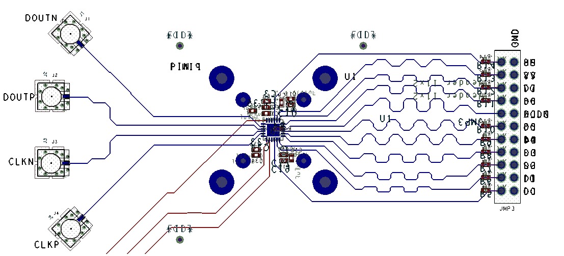 Figure 33. PCB Routing Example