SCES928B April 2021 – January 2024 SN74AXC2T45-Q1
PRODUCTION DATA
- 1
- 1 Features
- 2 Applications
- 3 Description
- 4 Pin Configuration and Functions
-
5 Specifications
- 5.1 Absolute Maximum Ratings
- 5.2 ESD Ratings
- 5.3 Recommended Operating Conditions
- 5.4 Thermal Information
- 5.5 Electrical Characteristics
- 5.6 Switching Characteristics, VCCA = 0.7 ± 0.05V
- 5.7 Switching Characteristics, VCCA = 0.8 ± 0.04V
- 5.8 Switching Characteristics, VCCA = 0.9 ± 0.045V
- 5.9 Switching Characteristics, VCCA = 1.2 ± 0.1V
- 5.10 Switching Characteristics, VCCA = 1.5 ± 0.1V
- 5.11 Switching Characteristics, VCCA = 1.8 ± 0.15V
- 5.12 Switching Characteristics, VCCA = 2.5 ± 0.2V
- 5.13 Switching Characteristics, VCCA = 3.3 ± 0.3V
- 5.14 Operating Characteristics: TA = 25°C
- 5.15 Typical Characteristics
- 6 Parameter Measurement Information
-
7 Detailed Description
- 7.1 Overview
- 7.2 Functional Block Diagram
- 7.3
Feature Description
- 7.3.1 Standard CMOS Inputs
- 7.3.2 Balanced High-Drive CMOS Push-Pull Outputs
- 7.3.3 Partial Power Down (Ioff)
- 7.3.4 VCC Isolation
- 7.3.5 Over-voltage Tolerant Inputs
- 7.3.6 Glitch-Free Power Supply Sequencing
- 7.3.7 Negative Clamping Diodes
- 7.3.8 Fully Configurable Dual-Rail Design
- 7.3.9 I/Os with Integrated Static Pull-Down Resistors
- 7.3.10 Supports High-Speed Translation
- 7.4 Device Functional Modes
- 8 Application and Implementation
- 9 Device and Documentation Support
- 10Mechanical, Packaging, and Orderable Information
- 11Revision History
Package Options
Refer to the PDF data sheet for device specific package drawings
Mechanical Data (Package|Pins)
- DCU|8
Thermal pad, mechanical data (Package|Pins)
Orderable Information
4 Pin Configuration and Functions
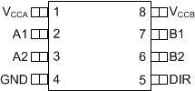 Figure 4-1 DCU Package,8-Pin VSSOP(Top View)
Table 4-1 Pin Functions
| PIN | TYPE(1) | DESCRIPTION | |
|---|---|---|---|
| NAME | NO. | ||
| A1 | 2 | I/O | Input/output A1. Referenced to VCCA. |
| A2 | 3 | I/O | Input/output A2. Referenced to VCCA. |
| B1 | 7 | I/O | Input/output B1. Referenced to VCCB. |
| B2 | 6 | I/O | Input/output B2. Referenced to VCCB. |
| DIR | 5 | Direction-control in for both ports. Referenced to VCCA | |
| GND | 4 | G | Ground |
| VCCA | 1 | P | A-port power supply voltage. 0.65V ≤ VCCA ≤ 3.6V |
| VCCB | 8 | P | B-port power supply voltage. 0.65V ≤ VCCB ≤ 3.6V |
(1) I = input, O = output, P = power, G = ground