SCES883C December 2018 – September 2020 SN74AXCH1T45
PRODUCTION DATA
- 1 Features
- 2 Applications
- 3 Description
- 4 Revision History
- 5 Pin Configuration and Functions
-
6 Specifications
- 6.1 Absolute Maximum Ratings
- 6.2 ESD Ratings
- 6.3 Recommended Operating Conditions
- 6.4 Thermal Information
- 6.5 Electrical Characteristics
- 6.6 Switching Characteristics, VCCA = 0.7 V
- 6.7 Switching Characteristics, VCCA = 0.8 V
- 6.8 Switching Characteristics, VCCA = 0.9 V
- 6.9 Switching Characteristics, VCCA = 1.2 V
- 6.10 Switching Characteristics, VCCA = 1.5 V
- 6.11 Switching Characteristics, VCCA = 1.8 V
- 6.12 Switching Characteristics, VCCA = 2.5 V
- 6.13 Switching Characteristics, VCCA = 3.3 V
- 6.14 Operating Characteristics: TA = 25°C
- 6.15 Typical Characteristics
- 7 Parameter Measurement Information
-
8 Detailed Description
- 8.1 Overview
- 8.2 Functional Block Diagram
- 8.3
Feature Description
- 8.3.1 Standard CMOS Inputs
- 8.3.2 Balanced High-Drive CMOS Push-Pull Outputs
- 8.3.3 Partial Power Down (Ioff)
- 8.3.4 VCC Isolation
- 8.3.5 Over-Voltage Tolerant Inputs
- 8.3.6 Negative Clamping Diodes
- 8.3.7 Fully Configurable Dual-Rail Design
- 8.3.8 Supports High-Speed Translation
- 8.3.9 Bus-Hold Data Inputs
- 8.4 Device Functional Modes
- 9 Application and Implementation
- 10Power Supply Recommendations
- 11Layout
- 12Device and Documentation Support
- 13Mechanical, Packaging, and Orderable Information
Package Options
Mechanical Data (Package|Pins)
Thermal pad, mechanical data (Package|Pins)
- DRY|6
Orderable Information
9.2.1 Interrupt Request Application
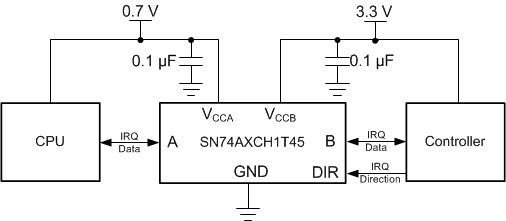
Figure 9-1 shows an example of the SN74AXCH1T45 being used in an application where a system controller flags an interrupt request (IRQ) to the CPU. The system controller determines the direction of the IRQ line to either flag an interrupt to the CPU or allow the CPU to drive data on the line. In this application the controller is operating at 3.3 V while the CPU can be operating as low as 0.65 V.
The SN74AXCH1T45 device is used to ensure that these devices can communicate at the appropriate voltage levels. Because the SN74AXCH1T45 does not have an output-enable ( OE) pin, the system designer should take precautions to avoid bus contention between the CPU and controller when changing directions.
 Figure 9-1 Interrupt Request Application