SCLS175H march 2003 – august 2023 SN54HCT244 , SN74HCT244
PRODUCTION DATA
- 1
- 1 Features
- 2 Applications
- 3 Description
- 4 Revision History
- 5 Pin Configuration and Functions
-
6 Specifications
- 6.1 Absolute Maximum Ratings
- 6.2 ESD Ratings
- 6.3 Recommended Operating Conditions
- 6.4 Thermal Information
- 6.5 Electrical Characteristics - SN54HCT244
- 6.6 Electrical Characteristics - SN74HCT244
- 6.7 Switching Characteristics: SN54HCT244
- 6.8 Switching Characteristics: SN74HCT244
- 6.9 Operating Characteristics
- 6.10 Typical Characteristics
- 7 Parameter Measurement Information
- 8 Detailed Description
- 9 Application and Implementation
- 10Device and Documentation Support
- 11Mechanical, Packaging, and Orderable Information
Package Options
Refer to the PDF data sheet for device specific package drawings
Mechanical Data (Package|Pins)
- DB|20
- NS|20
- N|20
- DGS|20
- DW|20
- PW|20
Thermal pad, mechanical data (Package|Pins)
Orderable Information
5 Pin Configuration and Functions
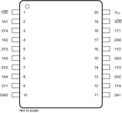
 J, DB, DW, N, NS, PW or DGS Packages, 20-Pin CDIP, CFP, SSOP, SOIC, PDIP, SO, TSSOP, or VSSOP (Top View)
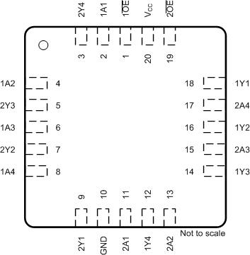
 FK Package, 20-Pin LCCC (Top View)
Table 5-1 Pin Functions
| PIN | TYPE(1) | DESCRIPTION | |
|---|---|---|---|
| NAME | NO. | ||
| 1 OE | 1 | I | Output enable |
| 1A1 | 2 | I | Input |
| 2Y4 | 3 | O | Output |
| 1A2 | 4 | I | Input |
| 2Y3 | 5 | O | Output |
| 1A3 | 6 | I | Input |
| 2Y2 | 7 | O | Output |
| 1A4 | 8 | I | Input |
| 2Y1 | 9 | O | Output |
| GND | 10 | — | Ground |
| 2A1 | 11 | I | Input |
| 1Y4 | 12 | O | Output |
| 2A2 | 13 | I | Input |
| 1Y3 | 14 | O | Output |
| 2A3 | 15 | I | Input |
| 1Y2 | 16 | O | Output |
| 2A4 | 17 | I | Input |
| 1Y1 | 18 | O | Output |
| 2 OE | 19 | I | Output enable |
| VCC | 20 | — | Power pin |
(1) Signal Types: I = Input, O = Output, I/O = Input or Output.