SCPS267B March 2017 – February 2020 TCA9803
PRODUCTION DATA.
- 1 Features
- 2 Applications
- 3 Description
- 4 Revision History
- 5 Device Comparison Table
- 6 Pin Configuration and Functions
- 7 Specifications
- 8 Parameter Measurement Information
-
9 Detailed Description
- 9.1 Overview
- 9.2 Functional Block Diagram
- 9.3
Feature Description
- 9.3.1 Integrated Current Source
- 9.3.2 Ultra-Low Power Consumption
- 9.3.3 No Static-Voltage Offset
- 9.3.4 Active-High Repeater Enable Input
- 9.3.5 Powered Off High Impedance I2C Bus Pins on A-Side
- 9.3.6 Powered-Off Back-Power Protection for I2C Bus Pins
- 9.3.7 Clock Stretching and Multiple Master Arbitration Support
- 9.4 Device Functional Modes
- 10Application and Implementation
- 11Power Supply Recommendations
- 12Layout
- 13Device and Documentation Support
- 14Mechanical, Packaging, and Orderable Information
Package Options
Mechanical Data (Package|Pins)
- DGK|8
Thermal pad, mechanical data (Package|Pins)
Orderable Information
10.2.4 Series Device Use Case
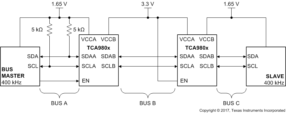
The TCA980x family supports multiple TCA980x used in series. It is acceptable to connect A sides together, or have A sides connect to B sides, but B-sides may never be connected together.
It is critical to note that there are no external sources of current allowed on the B-side ports, since this can affect device operation as shown in the IEXT-I section.
NOTE: B-sides of TCA980x devices may never be connected to each other, because the IEXT-I specification limit is violated. See the IEXT-I for more information.
NOTE: The B-side may not be connected to another translator if it uses a static-voltage offset. The RILC spec is violated since the static voltage offset adjusts the output resistance to ground to be outside of the RILC spec requirement, causing the TCA980x to be unable to recognize a low.
 Figure 34. Series Use Case
 NOTE
Decoupling capacitors are not shown to keep the illustration simple. Decoupling capacitors (1 µF and 0.1 µF) must be placed close to each power supply pin.