SCPS267B March 2017 – February 2020 TCA9803
PRODUCTION DATA.
- 1 Features
- 2 Applications
- 3 Description
- 4 Revision History
- 5 Device Comparison Table
- 6 Pin Configuration and Functions
- 7 Specifications
- 8 Parameter Measurement Information
-
9 Detailed Description
- 9.1 Overview
- 9.2 Functional Block Diagram
- 9.3
Feature Description
- 9.3.1 Integrated Current Source
- 9.3.2 Ultra-Low Power Consumption
- 9.3.3 No Static-Voltage Offset
- 9.3.4 Active-High Repeater Enable Input
- 9.3.5 Powered Off High Impedance I2C Bus Pins on A-Side
- 9.3.6 Powered-Off Back-Power Protection for I2C Bus Pins
- 9.3.7 Clock Stretching and Multiple Master Arbitration Support
- 9.4 Device Functional Modes
- 10Application and Implementation
- 11Power Supply Recommendations
- 12Layout
- 13Device and Documentation Support
- 14Mechanical, Packaging, and Orderable Information
Package Options
Mechanical Data (Package|Pins)
- DGK|8
Thermal pad, mechanical data (Package|Pins)
Orderable Information
7.8 Typical Characteristics
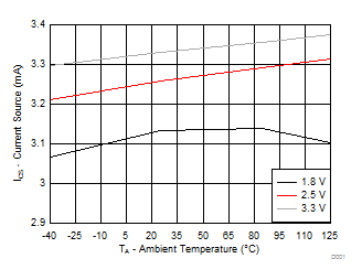 Figure 1. Current Source vs Ambient Temperature for Different VCCB
 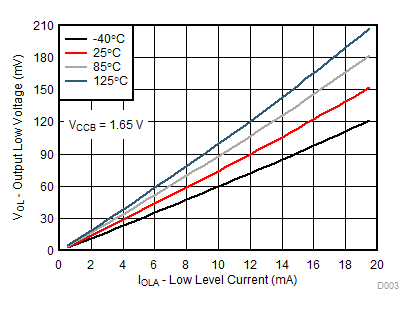 Figure 3. A-Side Output Low Voltage vs Low Level Current for Different TA (VCCB = 1.65 V)
 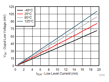 Figure 5. A-Side Output Low Voltage vs Low Level Current for Different TA (VCCB = 3.6 V)
 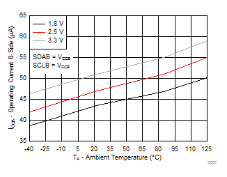 Figure 7. Operating Current B-Side vs Ambient Temperature for Different VCCB (B-Side = VCCB)
 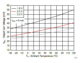 Figure 2. A-Side Output Low Voltage vs Ambient Temperature for Different VCCB (IOLA = 6 mA)
 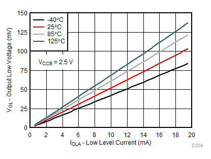 Figure 4. A-Side Output Low Voltage vs Low Level Current for Different TA (VCCB = 2.5 V)
 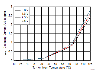 Figure 6. Operating Current A-Side vs Ambient Temperature for Different VCCA (A-Side = VCCA & GND)
 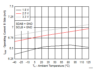 Figure 8. Operating Current B-Side vs Ambient Temperature for Different VCCB (B-Side = GND)