SLLSF91A December   2018  – January 2020 TCAN4550

PRODUCTION DATA.  

  1. Features
  2. Applications
  3. Description
    1.     Device Images
      1.      Simplified Schematics, CLKIN from MCU
      2.      Simplified Schematics, Crystal
  4. Revision History
  5. Pin Configuration and Functions
    1.     Pin Functions
  6. Specifications
    1. 6.1  Absolute Maximum Ratings
    2. 6.2  ESD Ratings
    3. 6.3  ESD Ratings, IEC ESD and ISO Transient Specification
    4. 6.4  Recommended Operating Conditions
    5. 6.5  Thermal Information
    6. 6.6  Supply Characteristics
    7. 6.7  Electrical Characteristics
    8. 6.8  Timing Requirements
    9. 6.9  Switching Characteristics
    10. 6.10 Typical Characteristics
  7. Parameter Measurement Information
  8. Detailed Description
    1. 8.1 Overview
    2. 8.2 Functional Block Diagram
    3. 8.3 Feature Description
      1. 8.3.1  VSUP Pin
      2. 8.3.2  VIO Pin
      3. 8.3.3  VCCOUT Pin
      4. 8.3.4  GND
      5. 8.3.5  INH Pin
      6. 8.3.6  WAKE Pin
      7. 8.3.7  FLTR Pin
      8. 8.3.8  RST Pin
      9. 8.3.9  OSC1 and OSC2 Pins
      10. 8.3.10 nWKRQ Pin
      11. 8.3.11 nINT Interrupt Pin
      12. 8.3.12 GPO1 Pin
      13. 8.3.13 GPO2 Pin
      14. 8.3.14 CANH and CANL Bus Pins
    4. 8.4 Device Functional Modes
      1. 8.4.1 Normal Mode
      2. 8.4.2 Standby Mode
      3. 8.4.3 Sleep Mode
        1. 8.4.3.1 Bus Wake via RXD_INT Request (BWRR) in Sleep Mode
        2. 8.4.3.2 Local Wake Up (LWU) via WAKE Input Terminal
      4. 8.4.4 Test Mode
      5. 8.4.5 Failsafe Feature
      6. 8.4.6 Protection Features
        1. 8.4.6.1 Watchdog Function
        2. 8.4.6.2 Driver and Receiver Function
        3. 8.4.6.3 Floating Terminals
        4. 8.4.6.4 TXD_INT Dominant Timeout (DTO)
        5. 8.4.6.5 CAN Bus Short Circuit Current Limiting
        6. 8.4.6.6 Thermal Shutdown
        7. 8.4.6.7 Under Voltage Lockout (UVLO) and Unpowered Device
          1. 8.4.6.7.1 UVSUP and UVCCOUT
          2. 8.4.6.7.2 UVIO
          3. 8.4.6.7.3 Fault and M_CAN Core Behavior:
      7. 8.4.7 CAN FD
    5. 8.5 Programming
      1. 8.5.1 SPI Communication
        1. 8.5.1.1 Chip Select Not (nCS):
        2. 8.5.1.2 SPI Clock Input (SCLK):
        3. 8.5.1.3 SPI Data Input (SDI):
        4. 8.5.1.4 SPI Data Output (SDO):
      2. 8.5.2 Register Descriptions
    6. 8.6 Register Maps
      1. 8.6.1 Device ID and Interrupt/Diagnostic Flag Registers: 16'h0000 to 16'h002F
        1. 8.6.1.1 DEVICE_ID1[31:0] (address = h0000) [reset = h4E414354]
          1. Table 10. Device ID Field Descriptions
        2. 8.6.1.2 DEVICE_ID2[31:0] (address = h0004) [reset = h30353534]
          1. Table 11. Device ID Field Descriptions
        3. 8.6.1.3 Revision (address = h0008) [reset = h00110201]
          1. Table 12. Revision Field Descriptions
        4. 8.6.1.4 Status (address = h000C) [reset = h0000000U]
          1. Table 13. Status Field Descriptions
      2. 8.6.2 Device Configuration Registers: 16'h0800 to 16'h08FF
        1. 8.6.2.1 Modes of Operation and Pin Configuration Registers (address = h0800) [reset = hC8000468]
          1. Table 15. Modes of Operation and Pin Configuration Registers Field Descriptions
        2. 8.6.2.2 Timestamp Prescalar (address = h0804) [reset = h00000002]
          1. Table 16. EMC Enhancement and Timestamp Prescalar Field Descriptions
        3. 8.6.2.3 Test Register and Scratch Pad (address = h0808) [reset = h00000000]
          1. Table 17. Test and Scratch Pad Register Field Descriptions
        4. 8.6.2.4 Test Register (address = h080C) [reset = h00000000]
          1. Table 18. Test Register Field Descriptions
      3. 8.6.3 Interrupt/Diagnostic Flag and Enable Flag Registers: 16'h0820/0824 and 16'h0830
        1. 8.6.3.1 Interrupts (address = h0820) [reset = h00100000]
          1. Table 19. Interrupts Field Descriptions
        2. 8.6.3.2 MCAN Interrupts (address = h0824) [reset = h00000000]
          1. Table 20. MCAN Interrupts Field Descriptions
        3. 8.6.3.3 Interrupt Enables (address = h0830 ) [reset = hFFFFFFFF]
          1. Table 21. Interrupt Enables Field Descriptions
      4. 8.6.4 CAN FD Register Set: 16'h1000 to 16'h10FF
        1. 8.6.4.1  Core Release Register (address = h1000) [reset = hrrrddddd]
          1. Table 25. Core Release Register Field Descriptions
        2. 8.6.4.2  Endian Register (address = h1004) [reset = h87654321]
          1. Table 26. Endian Register Field Descriptions
        3. 8.6.4.3  Customer Register (address = h1008) [reset = h00000000]
          1. Table 27. Customer Register Field Descriptions
        4. 8.6.4.4  Data Bit Timing & Prescaler (address = h100C) [reset = h0000A33]
          1. Table 28. Data Bit Timing & Prescaler Field Descriptions
        5. 8.6.4.5  Test Register (address = h1010 ) [reset = h00000000]
          1. Table 29. Test Register Field Descriptions
        6. 8.6.4.6  RAM Watchdog (address = h1014) [reset = h00000000]
          1. Table 30. RAM Watchdog Field Descriptions
        7. 8.6.4.7  Control Register (address = h1018) [reset = 0000 0019]
          1. Table 31. Control Register Field Descriptions
        8. 8.6.4.8  Nominal Bit Timing & Prescaler Register (address = h101C) [reset = h06000A03]
          1. Table 32. Nominal Bit Timing & Prescaler Register Field Descriptions
        9. 8.6.4.9  Timestamp Counter Configuration (address = h1020) [reset = h00000000]
          1. Table 33. Timestamp Counter Configuration Descriptions
        10. 8.6.4.10 Timestamp Counter Value (address = h1024) [reset = h00000000]
          1. Table 34. Timestamp Counter Value Field Descriptions
        11. 8.6.4.11 Timeout Counter Configuration (address = h1028) [reset = hFFFF0000]
          1. Table 35. Timeout Counter Configuration Field Descriptions
        12. 8.6.4.12 Timeout Counter Value (address = h102C) [reset = h0000FFFF]
          1. Table 36. Timeout Counter Value Field Descriptions
        13. 8.6.4.13 Reserved (address = h1030 - h103C) [reset = h00000000]
          1. Table 37. Reserved Field Descriptions
        14. 8.6.4.14 Error Counter Register (address = h1040) [reset = h00000000]
          1. Table 38. Error Counter Register Field Descriptions
        15. 8.6.4.15 Protocol Status Register (address = h1044) [reset = h00000707]
          1. Table 39. Protocol Status Register Field Descriptions
        16. 8.6.4.16 Transmitter Delay Compensation Register (address = h1048) [reset = h00000000]
          1. Table 40. Transmitter Delay Compensation Register Field Descriptions
        17. 8.6.4.17 Reserved (address = h104C) [reset = h00000000]
          1. Table 41. Reserved Field Descriptions
        18. 8.6.4.18 Interrupt Register (address = h1050) [reset = h00000000]
          1. Table 42. Interrupt Register Field Descriptions
        19. 8.6.4.19 Interrupt Enable (address = h1054) [reset = h00000000]
          1. Table 43. Interrupt Enable Field Descriptions
        20. 8.6.4.20 Interrupt Line Select (address = h1058) [reset = h00000000]
          1. Table 44. Interrupt Line Select Field Descriptions
        21. 8.6.4.21 Interrupt Line Enable (address = h105C) [reset = h00000000]
          1. Table 45. Interrupt Line Enable Field Descriptions
        22. 8.6.4.22 Reserved (address = h1060 - h107C) [reset = h00000000]
          1. Table 46. Reserved Field Descriptions
        23. 8.6.4.23 Global Filter Configuration (address = h1080) [reset = h00000000]
          1. Table 47. Global Filter Configuration Field Descriptions
        24. 8.6.4.24 Standard ID Filter Configuration (address = h1084) [reset = h00000000]
          1. Table 48. Standard ID Filter Configuration Field Descriptions
        25. 8.6.4.25 Extended ID Filter Configuration (address = h1088) [reset = h00000000]
          1. Table 49. Extended ID Filter Configuration Field Descriptions
        26. 8.6.4.26 Reserved (address = h108C) [reset = h00000000]
          1. Table 50. Reserved Field Descriptions
        27. 8.6.4.27 Extended ID AND Mask (address = h1090) [reset = h1FFFFFFF]
          1. Table 51. Extended ID AND Mask Field Descriptions
        28. 8.6.4.28 High Priority Message Status (address = h1094) [reset = h00000000]
          1. Table 52. High Priority Message Status Field Descriptions
        29. 8.6.4.29 New Data 1 (address = h1098) [reset = h00000000]
          1. Table 53. New Data 1 Field Descriptions
        30. 8.6.4.30 New Data 2 (address = h109C) [reset = h00000000]
          1. Table 54. New Data 2 Field Descriptions
        31. 8.6.4.31 Rx FIFO 0 Configuration (address = h10A0) [reset = h00000000]
          1. Table 55. Rx FIFO 0 Configuration Field Descriptions
        32. 8.6.4.32 Rx FIFO 0 Status (address = h10A4) [reset = h00000000]
          1. Table 56. Rx FIFO 0 Status Field Descriptions
        33. 8.6.4.33 Rx FIFO 0 Acknowledge (address = h10A8) [reset = h00000000]
          1. Table 57. Rx FIFO 0 Acknowledge Field Descriptions
        34. 8.6.4.34 Rx Buffer Configuration (address = h10AC) [reset = h00000000]
          1. Table 58. Rx Buffer Configuration Field Descriptions
        35. 8.6.4.35 Rx FIFO 1 Configuration (address = h10B0) [reset = h00000000]
          1. Table 59. Rx FIFO 1 Configuration Field Descriptions
        36. 8.6.4.36 Rx FIFO 1 Status (address = h10B4) [reset = h00000000]
          1. Table 60. Rx FIFO 1 Status Field Descriptions
        37. 8.6.4.37 Rx FIFO 1 Acknowledge (address = h10B8) [reset = h00000000]
          1. Table 61. Rx FIFO 1 Acknowledge Field Descriptions
        38. 8.6.4.38 Rx Buffer/FIFO Element Size Configuration (address = h10BC) [reset = h00000000]
          1. Table 62. Rx Buffer/FIFO Element Size Configuration Field Descriptions
        39. 8.6.4.39 Tx Buffer Configuration (address = h10C0) [reset = h00000000]
          1. Table 63. Tx Buffer Configuration Field Descriptions
        40. 8.6.4.40 Tx FIFO/Queue Status (address = h10C4) [reset = h00000000]
          1. Table 64. Tx FIFO/Queue Status Field Descriptions
        41. 8.6.4.41 Tx Buffer Element Size Configuration (address = h10C8) [reset = h00000000]
          1. Table 65. Tx Buffer Element Size Configuration Field Descriptions
        42. 8.6.4.42 Tx Buffer Request Pending (address = h10CC) [reset = h00000000]
          1. Table 66. Tx Buffer Request Pending Field Descriptions
        43. 8.6.4.43 Tx Buffer Add Request (address = h10D0) [reset = h00000000]
          1. Table 67.   Tx Buffer Add Request Field Descriptions
          2. 8.6.4.43.1  Tx Buffer Cancellation Request (address = h10D4 [reset = h00000000]
            1. Table 68. Tx Buffer Cancellation Request Field Descriptions
          3. 8.6.4.43.2  Tx Buffer Add Request Transmission Occurred (address = h10D8) [reset = h00000000]
            1. Table 69. Tx Buffer Add Request Transmission Occurred Field Descriptions
          4. 8.6.4.43.3  Tx Buffer Cancellation Finished (address = h10DC) [reset = h00000000]
            1. Table 70. Tx Buffer Cancellation Finished Field Descriptions
          5. 8.6.4.43.4  Tx Buffer Transmission Interrupt Enable (address = h10E0) [reset = h00000000]
            1. Table 71. Tx Buffer Transmission Interrupt Enable Field Descriptions
          6. 8.6.4.43.5  Tx Buffer Cancellation Finished Interrupt Enable (address = h10E4) [reset = h00000000]
            1. Table 72. Tx Buffer Cancellation Finished Interrupt Enable Field Descriptions
          7. 8.6.4.43.6  Reserved (address = h10E8) [reset = h00000000]
            1. Table 73. Reserved Field Descriptions
          8. 8.6.4.43.7  Reserved (address = h10EC) [reset = h00000000]
            1. Table 74. Reserved Field Descriptions
          9. 8.6.4.43.8  Tx Event FIFO Configuration (address = h10F0) [reset = h00000000]
            1. Table 75. Tx Event FIFO Configuration Field Descriptions
          10. 8.6.4.43.9  Tx Event FIFO Status (address = h10F4) [reset = h00000000]
            1. Table 76. Tx Event FIFO Status Field Descriptions
          11. 8.6.4.43.10 Tx Event FIFO Acknowledge (address = h10F8) [reset = h00000000]
            1. Table 77. Tx Event FIFO Acknowledge Field Descriptions
          12. 8.6.4.43.11 Reserved (address = h10FC) [reset = h00000000]
            1. Table 78. Reserved Field Descriptions
  9. Application and Implementation
    1. 9.1 Application Design Consideration
      1. 9.1.1 Crystal and Clock Input Requirements
      2. 9.1.2 Bus Loading, Length and Number of Nodes
      3. 9.1.3 CAN Termination
        1. 9.1.3.1 Termination
        2. 9.1.3.2 CAN Bus Biasing
      4. 9.1.4 INH Brownout Behavior
    2. 9.2 Typical Application
      1. 9.2.1 Detailed Requirements
      2. 9.2.2 Detailed Design Procedures
      3. 9.2.3 Application Curves
      4. 9.2.4 Application Curves
  10. 10Power Supply Recommendations
  11. 11Layout
    1. 11.1 Layout Guidelines
    2. 11.2 Layout Example
  12. 12Device and Documentation Support
    1. 12.1 Documentation Support
      1. 12.1.1 Related Documentation
        1. 12.1.1.1 CAN Transceiver Physical Layer Standards:
        2. 12.1.1.2 EMC requirements:
        3. 12.1.1.3 Conformance Test requirements:
        4. 12.1.1.4 Support Documents
    2. 12.2 Receiving Notification of Documentation Updates
    3. 12.3 Support Resources
    4. 12.4 Trademarks
    5. 12.5 Electrostatic Discharge Caution
    6. 12.6 Glossary
  13. 13Mechanical, Packaging, and Orderable Information

Package Options

Mechanical Data (Package|Pins)
Thermal pad, mechanical data (Package|Pins)
Orderable Information

Parameter Measurement Information

NOTE

All TXD_INT, RXD_INT and EN_INT references are for internal nodes that represent the same functions for a physical layer transceiver. In test mode these can be brought out to pins to test the transceiver or CAN FD controller.
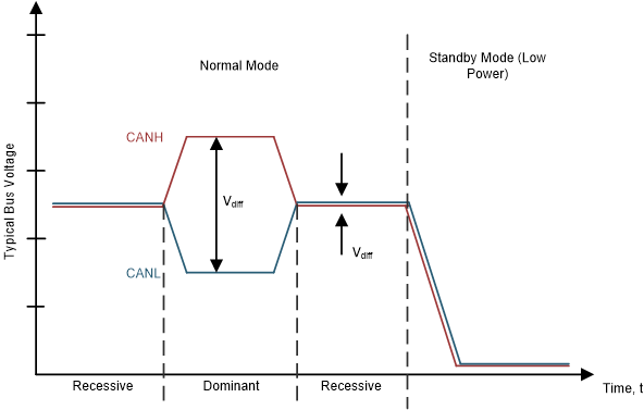
TCAN4550 sllsez5_bus_states_physical_bit_rep.gifFigure 3. Bus States (Physical Bit Representation)
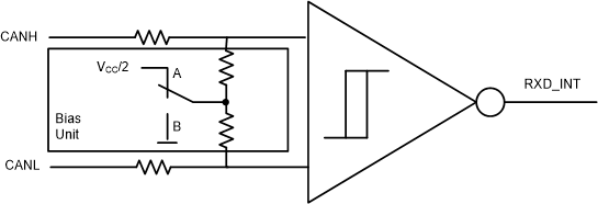
TCAN4550 sllsez5_simplified_recessive_common.gifFigure 4. Simplified Recessive Common Mode Bias Unit and Receiver

NOTE

A: Classic CAN and CAN FD modes

B: Standby and Sleep Modes (Low Power)
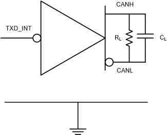
TCAN4550 sllsez5_supply_test_circuit.gifFigure 5. Supply Test Circuit
TCAN4550 sllsez5_driver_test_circuit_and_mea.gifFigure 6. Driver Test Circuit and Measurement
TCAN4550 sllsez5_receiver_test_circuit_and_m.gifFigure 7. Receiver Test Circuit and Measurement
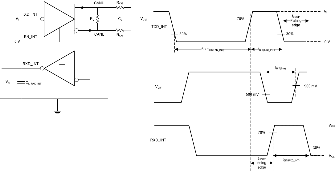
TCAN4550 sllsez5_transmitter_and_receiver_ti.gifFigure 8. Transmitter and Receiver Timing Behavior Test Circuit and Measurement
TCAN4550 sllsez5_txd_int_dominant_time_out_t.gifFigure 9. TXD_INT Dominant Timeout Test Circuit and Measurement
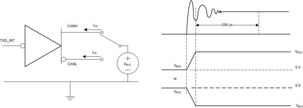
TCAN4550 sllsez5_driver_short_circuit_curren.gifFigure 10. Driver Short-Circuit Current Test and Measurement
TCAN4550 sllsez5_twake_while_monitoring_inh_.gifFigure 11. tWAKE While Monitoring INH Output
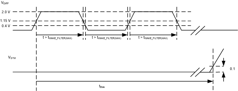
TCAN4550 sllsez5_test_sig_def_bias_reaction.gifFigure 12. Test Signal Definition for Bias Reaction Time Measurement
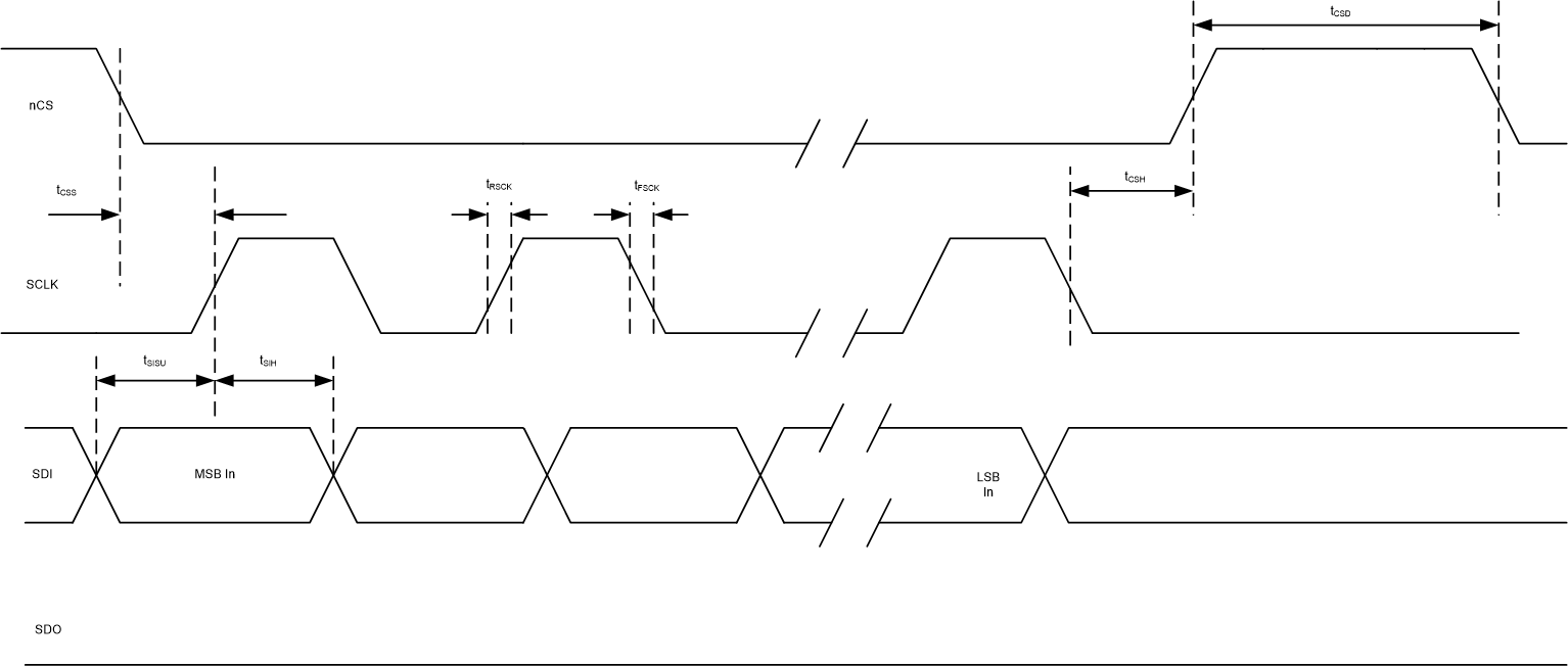
TCAN4550 sllsez5_spi_ac_char_write.gifFigure 13. SPI AC Characteristic Write
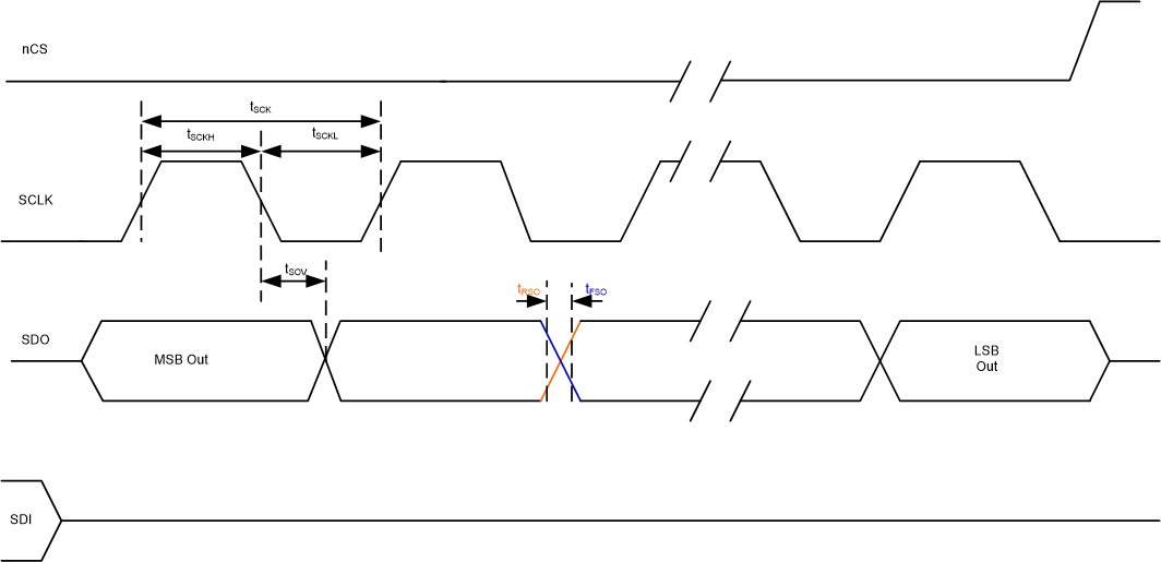
TCAN4550 sllsez5_spi_ac_char_read.gifFigure 14. SPI AC Characteristic Read
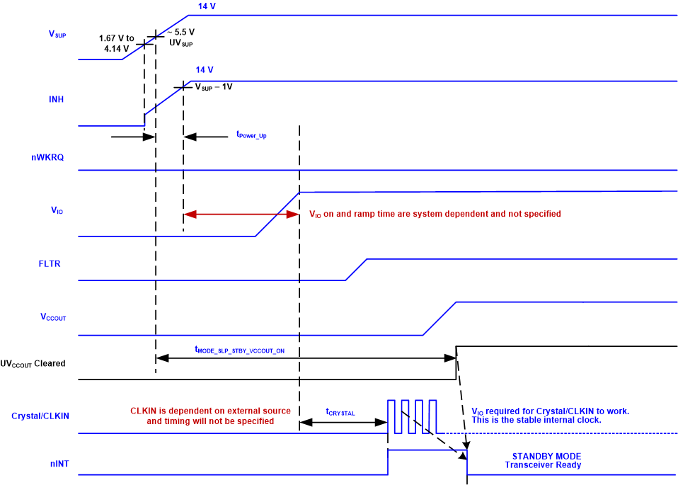
TCAN4550 sllsez5_sllsf45_power_up_timing.gifFigure 15. Power Up Timing
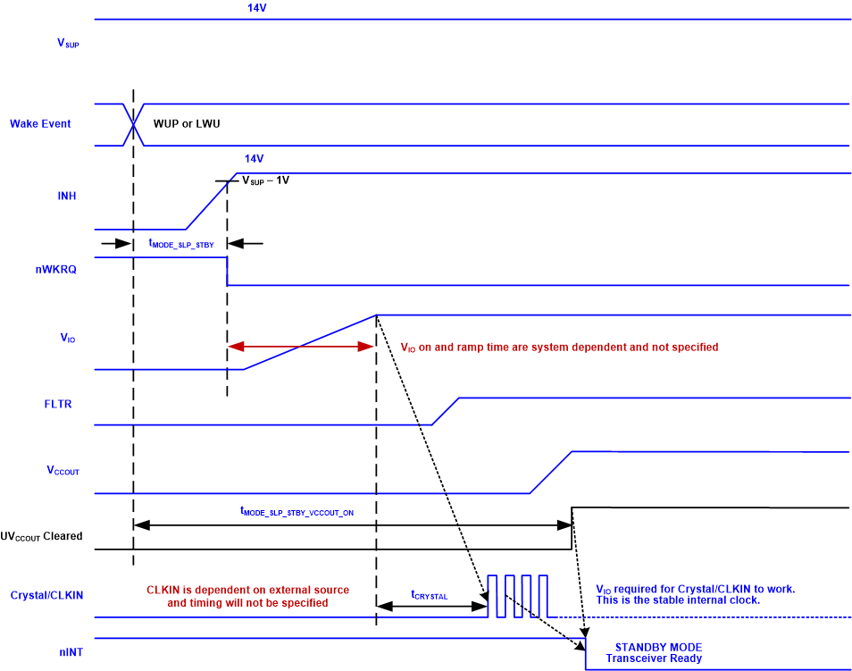
TCAN4550 sllsez5_sllsf45_slp_stdby_timing.gifFigure 16. Sleep to Standby Timing
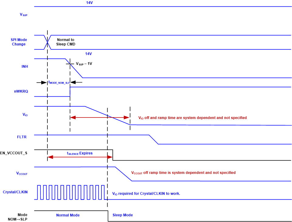
TCAN4550 sllsez5_sllsf45_norm_slp_timing.gifFigure 17. Normal to Sleep Timing
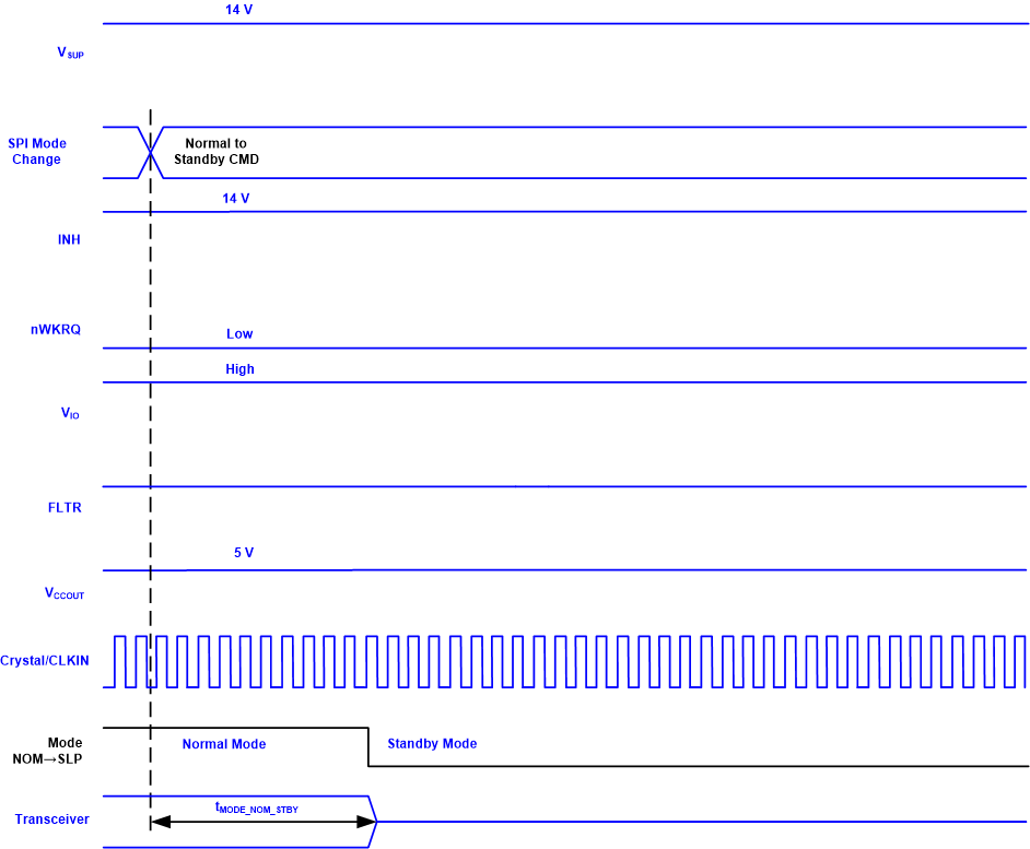
TCAN4550 sllsez5_sllsf45_norm_stby_timing.gifFigure 18. Normal to Standby Timing