SBOS932C January   2020  – March 2021 THP210

PRODUCTION DATA  

  1. Features
  2. Applications
  3. Description
  4. Revision History
  5. Pin Configuration and Functions
  6. Specifications
    1. 6.1 Absolute Maximum Ratings
    2. 6.2 ESD Ratings
    3. 6.3 Recommended Operating Conditions
    4. 6.4 Thermal Information
    5. 6.5 Electrical Characteristics
    6. 6.6 Typical Characteristics
  7. Parameter Measurement Information
    1. 7.1 Characterization Configuration
  8. Detailed Description
    1. 8.1 Overview
    2. 8.2 Functional Block Diagram
    3. 8.3 Feature Description
      1. 8.3.1 Super-Beta Input Bipolar Transistors
      2. 8.3.2 Power Down
      3. 8.3.3 Flexible Gain Setting
      4. 8.3.4 Amplifier Overload Power Limit
      5. 8.3.5 Unity Gain Stability
    4. 8.4 Device Functional Modes
  9. Application and Implementation
    1. 9.1 Application Information
      1. 9.1.1 I/O Headroom Considerations
      2. 9.1.2 DC Precision Analysis
        1. 9.1.2.1 DC Error Voltage at Room Temperature
        2. 9.1.2.2 DC Error Voltage Over Temperature
      3. 9.1.3 Noise Analysis
      4. 9.1.4 Mismatch of External Feedback Network
      5. 9.1.5 Operating the Power-Down Feature
      6. 9.1.6 Driving Capacitive Loads
      7. 9.1.7 Driving Differential ADCs
        1. 9.1.7.1 RC Filter Selection (Charge Kickback Filter)
        2. 9.1.7.2 Settling Time Driving the ADC Sample-and-Hold Operating Behavior
        3. 9.1.7.3 THD Performance
    2. 9.2 Typical Applications
      1. 9.2.1 MFB Filter
        1. 9.2.1.1 Design Requirements
        2. 9.2.1.2 Detailed Design Procedure
        3. 9.2.1.3 Application Curve
      2. 9.2.2 ADS891x With Single-Ended RC Filter Stage
        1. 9.2.2.1 Design Requirements
          1. 9.2.2.1.1 Measurement Results
      3. 9.2.3 Attenuation Configuration Drives the ADS8912B
        1. 9.2.3.1 Design Requirements
          1. 9.2.3.1.1 Measurement Results
  10. 10Power Supply Recommendations
  11. 11Layout
    1. 11.1 Layout Guidelines
      1. 11.1.1 Board Layout Recommendations
    2. 11.2 Layout Example
  12. 12Device and Documentation Support
    1. 12.1 Device Support
      1. 12.1.1 Development Support
    2. 12.2 Documentation Support
      1. 12.2.1 Related Documentation
    3. 12.3 Receiving Notification of Documentation Updates
    4. 12.4 Support Resources
    5. 12.5 Trademarks
    6. 12.6 Electrostatic Discharge Caution
    7. 12.7 Glossary
  13. 13Mechanical, Packaging, and Orderable Information

Package Options

Mechanical Data (Package|Pins)
Thermal pad, mechanical data (Package|Pins)
Orderable Information

ADS891x With Single-Ended RC Filter Stage

The application circuit in Figure 9-12 shows the schematic of a complete reference driver circuit that generates a full-scale range of 4.5 V at the ADC using a unipolar supply voltage of 5 V. This circuit is used to measure the driving capability of the THP210 with the different variants of the ADS891x ADC.

To test the complete dynamic range of the circuit, the common-mode voltage VOCM of the input of the ADC is established at a value of VREF / 2. To exclude distortion caused by reference voltage VREF and common-mode voltage VOCM of the ADC, the test circuit uses the low-noise OPA2625 in an inverting gain configuration for VOCM, and the high-precision, low-noise REF5050 for VREF. See the ADS8910BEVM-PDK user's guide for more details.
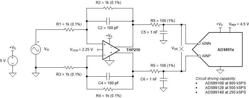
GUID-20200821-CA0I-BT41-VVXM-RBMFCW6KRKGB-low.gif Figure 9-12 Driving ADS891x With Single-Ended RC Filter Stage