SBOS932C January 2020 – March 2021 THP210
PRODUCTION DATA
- 1 Features
- 2 Applications
- 3 Description
- 4 Revision History
- 5 Pin Configuration and Functions
- 6 Specifications
- 7 Parameter Measurement Information
- 8 Detailed Description
-
9 Application and Implementation
- 9.1 Application Information
- 9.2 Typical Applications
- 10Power Supply Recommendations
- 11Layout
- 12Device and Documentation Support
- 13Mechanical, Packaging, and Orderable Information
Package Options
Mechanical Data (Package|Pins)
Thermal pad, mechanical data (Package|Pins)
Orderable Information
9.1.3 Noise Analysis
An accurate output-noise calculation allows the designer to compare the performance of alternate FDA solutions. The combination of differential spot noise at the output pins of the FDA with any passive filtering to the ADC enables an accurate signal-to-noise ratio (SNR) calculation. This chapter incorporates key elements for an output noise analysis.
The first step in the output noise analysis is to reduce the application circuit to the simplest form with equal feedback and gain setting elements to ground. Figure 9-4 shows the simplest analysis circuit with the FDA. This circuit considers the thermal resistor noise terms of the external feedback network and the intrinsic input voltage and current noise terms.
 Figure 9-4 FDA Noise Analysis
Circuit
Figure 9-4 FDA Noise Analysis
CircuitThe noise powers are shown in Figure 9-4 for each term. When the RF and RG (or RI) terms are matched on each side, the total differential output noise is the root sum squared (RSS) of these separate terms.
Using NG ≡ 1 + RF / RG as the noise gain, the total output noise density is given by Equation 3. Each resistor noise term is a 4kT × R power (4kT = 1.6E-20 J at 290 K).
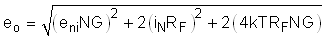
where:
- eni is the differential input spot noise times the noise gain.
- in x RF is
the input current noise terms times the feedback resistor.
Because there are two uncorrelated current noise terms, the power is two times one of them. - enRF is the thermal output noise resulting from both the RF and RG resistors at twice the value for the output noise power of each side added together.
Figure 9-5 and Figure 9-6 provide a graphical comparison of the described noise densities versus different gain settings. Each of the contributors are separately showcased in the graphs. As expected, lower feedback resistors (in this case, 2 kΩ) show that the dominant factor of the total output noise is the intrinsic voltage noise of the FDA (at gains > 2). For smaller gain settings, the thermal noise of the feedback resistors is dominating.

| RF = 2 kΩ |
vs Gain Settings

| RF = 10 kΩ |
vs Gain Settings
The advancement of the THP210 can be seen at higher feedback resistors (in this case 10 kΩ). Many FDAs exhibit an input current noise density in the range of some pA/√Hz that, in cases for higher feedback resistors, dictate the noise behavior. As a result of the superior current noise density of 300 fA/√Hz of the THP210, the overall output noise is mainly dominated by the thermal noise of the resistors (here, up to gains of approximately 15).
The total output voltage noise density is important when using FDAs as ADC input driver stages. To evaluate the compatibility between the input driver and the ADC from a noise perspective, compare the calculated RMS output noise of the FDA with the least-significant bit (LSB) of the desired ADC application, in respect to the effective number of bits (ENOB). Section 9.2.2 shows measurements of the THP210 in combination with state-of-the-art SAR ADCs, and indicates the performance that is achieved.