SBOS932C January 2020 – March 2021 THP210
PRODUCTION DATA
- 1 Features
- 2 Applications
- 3 Description
- 4 Revision History
- 5 Pin Configuration and Functions
- 6 Specifications
- 7 Parameter Measurement Information
- 8 Detailed Description
-
9 Application and Implementation
- 9.1 Application Information
- 9.2 Typical Applications
- 10Power Supply Recommendations
- 11Layout
- 12Device and Documentation Support
- 13Mechanical, Packaging, and Orderable Information
Package Options
Mechanical Data (Package|Pins)
Thermal pad, mechanical data (Package|Pins)
Orderable Information
9.1.7.1 RC Filter Selection (Charge Kickback Filter)
The sample-and-hold operating behavior of SAR ADCs causes charge transients at the input stage, and thus to the output stage of the amplifier. The RC filter helps to attenuate the sampling charge injection from the switched capacitor input stage of the ADC. A careful design is critical to meet linearity and noise performance of the ADC.
Figure 9-8 and Figure 9-9 show a single-ended and differential filter approach, respectively.
 Figure 9-8 Single-Ended
Filter
Figure 9-8 Single-Ended
Filter Figure 9-9 Differential
Filter
Figure 9-9 Differential
FilterChoose the capacitor to be at least 10 times larger than the specified value of the SAR ADC sampling capacitor. A trade-off must be considered for the isolation resistor, where a higher damping effect is achieved at higher values, and lower value provide better THD at the input of the ADC. To select the best RC combination, use the Analog Engineering Tool.
One important element to consider is that the small-signal bandwidth of the FDA (fSSBW_FDA) determines what the cutoff frequency of the RC filter combination can be driven at the inputs of the ADC. Depending whether a single-ended filter or a differential filter is used the minimum required small-signal bandwidth of the FDA (fSSBW_FDA) can be estimated by Equation 4:
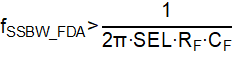
where:
- SEL = 1 for single-ended filter, SEL = 2 for differential filter
Driving higher capacitive loads degrades the phase margin of the FDA, and causes instability issues. Best practice is to perform a SPICE simulation using TINA-TI™ simulation software to confirm that the desired circuit is stable; that is, the FDA has more than a 45° phase margin.