SBOS875C August 2017 – February 2023 THS3491
PRODUCTION DATA
- 1 Features
- 2 Applications
- 3 Description
- 4 Revision History
- 5 Device Comparison Table
- 6 Pin Configuration and Functions
- 7 Bare Die Information
- 8 Specifications
- 9 Detailed Description
- 10Application and Implementation
- 11Device and Documentation Support
- 12Mechanical, Packaging, and Orderable Information
Package Options
Mechanical Data (Package|Pins)
Thermal pad, mechanical data (Package|Pins)
Orderable Information
9.4.1 Wideband Noninverting Operation
The THS3491 is a 900-MHz current-feedback operational amplifier that is designed to operate from a power supply of ±7 V to ±16 V.
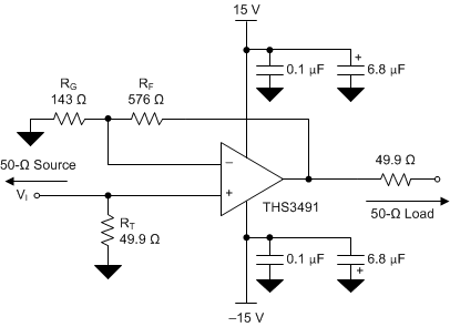
#SLOS420FIG3931 shows the THS3491 in a noninverting gain configuration of 5 V/V which is used to generate the majority of the performance curves. Most of the curves are characterized using signal sources with a 50-Ω source impedance and measurement equipment presenting a 50-Ω load impedance.
 Figure 9-1 Wideband Noninverting Gain Configuration (5 V/V)
Current-feedback amplifiers are highly dependent on the RF feedback resistor for maximum performance and stability. Table 9-2 provides the optimal resistor values for RF and RG at different gains to achieve maximum bandwidth with minimal peaking in the frequency response. Use lower RF values for higher bandwidth. Note that this can cause additional peaking and a reduction in phase margin. Conversely, increasing RF decreases the bandwidth but phase margin increases and stability improves. To gain further insight on the feedback and stability analysis of current-feedback amplifiers like the THS3491, see the Current-feedback Amplifiers section of TI Precision Labs.
With RLOAD = 100 Ω
| GAIN (V/V) | RGT PACKAGE | DDA PACKAGE | ||
|---|---|---|---|---|
| RG (Ω) | RF (Ω) | RG (Ω) | RF (Ω) | |
| 2 | 976 | 976 | 2.1k | 2.1k |
| 5 | 143 | 576 | 200 | 798 |
| 10 | 54.9 | 499 | 78.7 | 704 |
| 20 | 20 | 383 | 29.4 | 564 |