SBOS875C August   2017  – February 2023 THS3491

PRODUCTION DATA  

  1. Features
  2. Applications
  3. Description
  4. Revision History
  5. Device Comparison Table
  6. Pin Configuration and Functions
  7. Bare Die Information
  8. Specifications
    1. 8.1 Absolute Maximum Ratings
    2. 8.2 ESD Ratings
    3. 8.3 Recommended Operating Conditions
    4. 8.4 Thermal Information
    5. 8.5 Electrical Characteristics: VS = ±15 V
    6. 8.6 Electrical Characteristics: VS = ±7.5 V
    7. 8.7 Typical Characteristics: ±15 V
    8. 8.8 Typical Characteristics: ±7.5 V
  9. Detailed Description
    1. 9.1 Overview
    2. 9.2 Functional Block Diagram
    3. 9.3 Feature Description
      1. 9.3.1 Power-Down (PD) Pin
      2. 9.3.2 Power-Down Reference (REF) Pin
      3. 9.3.3 Internal Junction Temperature Sense (TJ_SENSE) Pin
    4. 9.4 Device Functional Modes
      1. 9.4.1 Wideband Noninverting Operation
      2. 9.4.2 Wideband, Inverting Operation
      3. 9.4.3 Single-Supply Operation
      4. 9.4.4 Maximum Recommended Output Voltage
  10. 10Application and Implementation
    1. 10.1 Application Information
      1. 10.1.1 Driving Capacitive Loads
      2. 10.1.2 Video Distribution
    2. 10.2 Typical Application
      1. 10.2.1 Design Requirements
      2. 10.2.2 Detailed Design Procedure
      3. 10.2.3 Application Curves
    3. 10.3 Power Supply Recommendations
    4. 10.4 Layout
      1. 10.4.1 Layout Guidelines
        1. 10.4.1.1 PowerPAD™ Integrated Circuit Package Design Considerations (DDA Package Only)
          1. 10.4.1.1.1 PowerPAD™ Integrated Circuit Package Layout Considerations
          2. 10.4.1.1.2 Power Dissipation and Thermal Considerations
      2. 10.4.2 Layout Example
  11. 11Device and Documentation Support
    1. 11.1 Documentation Support
      1. 11.1.1 Related Documentation
    2. 11.2 Receiving Notification of Documentation Updates
    3. 11.3 Support Resources
    4. 11.4 Trademarks
    5. 11.5 Electrostatic Discharge Caution
    6. 11.6 Glossary
  12. 12Mechanical, Packaging, and Orderable Information

Package Options

Mechanical Data (Package|Pins)
Thermal pad, mechanical data (Package|Pins)
Orderable Information

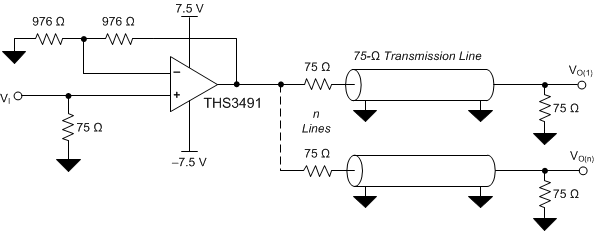
Video Distribution

The wide bandwidth, high slew rate, and high output drive current of the THS3491 meets the demands for video distribution by delivering video signals down multiple cables. For high signal quality with minimal degradation of performance, use a 0.1-dB gain flatness that is at least seven times the pass-band frequency to minimize group delay variations from the amplifier. A high slew rate minimizes distortion of the video signal and supports component video and RGB video signals that require fast transition and settling times for high signal quality.
GUID-090995BF-B39B-4A25-BF65-79426B4FBC0C-low.gifFigure 10-4 Video Distribution Amplifier Application