SBOS875C August   2017  – February 2023 THS3491

PRODUCTION DATA  

  1. Features
  2. Applications
  3. Description
  4. Revision History
  5. Device Comparison Table
  6. Pin Configuration and Functions
  7. Bare Die Information
  8. Specifications
    1. 8.1 Absolute Maximum Ratings
    2. 8.2 ESD Ratings
    3. 8.3 Recommended Operating Conditions
    4. 8.4 Thermal Information
    5. 8.5 Electrical Characteristics: VS = ±15 V
    6. 8.6 Electrical Characteristics: VS = ±7.5 V
    7. 8.7 Typical Characteristics: ±15 V
    8. 8.8 Typical Characteristics: ±7.5 V
  9. Detailed Description
    1. 9.1 Overview
    2. 9.2 Functional Block Diagram
    3. 9.3 Feature Description
      1. 9.3.1 Power-Down (PD) Pin
      2. 9.3.2 Power-Down Reference (REF) Pin
      3. 9.3.3 Internal Junction Temperature Sense (TJ_SENSE) Pin
    4. 9.4 Device Functional Modes
      1. 9.4.1 Wideband Noninverting Operation
      2. 9.4.2 Wideband, Inverting Operation
      3. 9.4.3 Single-Supply Operation
      4. 9.4.4 Maximum Recommended Output Voltage
  10. 10Application and Implementation
    1. 10.1 Application Information
      1. 10.1.1 Driving Capacitive Loads
      2. 10.1.2 Video Distribution
    2. 10.2 Typical Application
      1. 10.2.1 Design Requirements
      2. 10.2.2 Detailed Design Procedure
      3. 10.2.3 Application Curves
    3. 10.3 Power Supply Recommendations
    4. 10.4 Layout
      1. 10.4.1 Layout Guidelines
        1. 10.4.1.1 PowerPAD™ Integrated Circuit Package Design Considerations (DDA Package Only)
          1. 10.4.1.1.1 PowerPAD™ Integrated Circuit Package Layout Considerations
          2. 10.4.1.1.2 Power Dissipation and Thermal Considerations
      2. 10.4.2 Layout Example
  11. 11Device and Documentation Support
    1. 11.1 Documentation Support
      1. 11.1.1 Related Documentation
    2. 11.2 Receiving Notification of Documentation Updates
    3. 11.3 Support Resources
    4. 11.4 Trademarks
    5. 11.5 Electrostatic Discharge Caution
    6. 11.6 Glossary
  12. 12Mechanical, Packaging, and Orderable Information

Package Options

Mechanical Data (Package|Pins)
Thermal pad, mechanical data (Package|Pins)
Orderable Information

Maximum Recommended Output Voltage

The THS3491 is designed to produce better than 40 dB SFDR while driving a 100-MHz, 20-Vpp signal into a 100-Ω load. To accomplish this, the geometries of certain signal path transistors must be limited. As a result of this limitation, some internal devices begin to saturate when large signal levels are input at frequencies greater than 100 MHz. When these devices saturate, the loop opens and the amplifier is no longer in linear operation. This appears as a gain step-up in the frequency response curve. To avoid this phenomenon, applications must comply with the recommended linear operating region shown in #T4901919-62. #T4901919-62 shows the maximum output voltage vs frequency that is permitted to keep the amplifier in linear operation.
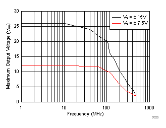
GUID-C2F54C45-73F6-456A-A229-B2B58F55A7EA-low.gifFigure 9-4 Maximum Recommended Output Voltage vs Frequency