SBOS974D August 2019 – April 2021 THS6222
PRODUCTION DATA
- 1 Features
- 2 Applications
- 3 Description
- 4 Revision History
- 5 Pin Configuration and Functions
- 6 Specifications
- 7 Detailed Description
- 8 Application and Implementation
- 9 Power Supply Recommendations
- 10Layout
- 11Device and Documentation Support
- 12Mechanical, Packaging, and Orderable Information
Package Options
Mechanical Data (Package|Pins)
Thermal pad, mechanical data (Package|Pins)
- RGT|16
Orderable Information
5 Pin Configuration and Functions

NC = no
internal connection.
Figure 5-1 RHF Package24-Pin VQFN With Exposed Thermal Pad
Top View
 Figure 5-2 RGT Package
16-Pin VQFN With Exposed Thermal Pad
Top View
Table 5-1 Pin Functions
| PIN | TYPE(1) | DESCRIPTION | ||
|---|---|---|---|---|
| NAME | RHF | RGT | ||
| BIAS-1(2) | 23 | 15 | I | Bias mode control, LSB |
| BIAS-2(2) | 24 | 16 | I | Bias mode control, MSB |
| D1_IN– | 19 | 11 | I | Amplifier D1 inverting input |
| D2_IN– | 18 | 10 | I | Amplifier D2 inverting input |
| D1_IN+ | 1 | 1 | I | Amplifier D1 noninverting input |
| D2_IN+ | 2 | 2 | I | Amplifier D2 noninverting input |
| D1_OUT | 20 | 12 | O | Amplifier D1 output |
| D2_OUT | 17 | 9 | O | Amplifier D2 output |
| DGND(3) | 3 | 3 | I | Ground reference for bias control pins |
| IADJ | 4 | 4 | I | Bias current adjustment pin |
| NC | 6-16 | 6 | — | No internal connection |
| VCM | 5 | 5 | O | Common-mode buffer output |
| VS– | 22 | 7, 14 | P | Negative power-supply connection |
| VS+ | 21 | 8, 13 | P | Positive power-supply connection |
| Thermal Pad | P | Electrically connected to die substrate and VS–. Connect to VS– on the printed circuit board (PCB) for best performance. | ||
(1) I = input, O = output, and P = power,
(2) The THS6222 defaults to the
shutdown (disable) state if a signal is not present on the bias pins.
(3) The DGND pin ranges from VS– to (VS+ – 5 V).
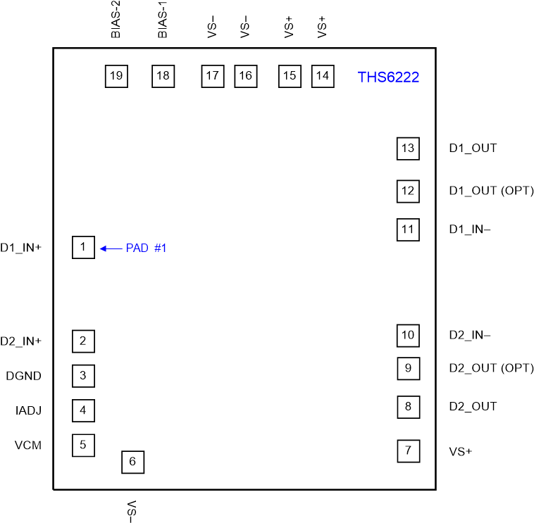
 Figure 5-3 YS Die
19-Pad Wafer Sale
Top View
Bond Pad Functions
| PAD | Type(1) | DESCRIPTION | |
|---|---|---|---|
| NAME | NO. | ||
| BIAS-1(2) | 18 | I | Bias mode parallel control, LSB |
| BIAS-2(2) | 19 | I | Bias mode parallel control, MSB |
| D1_IN– | 11 | I | Amplifier D1 inverting input |
| D2_IN– | 10 | I | Amplifier D2 inverting input |
| D1_IN+ | 1 | I | Amplifier D1 noninverting input |
| D2_IN+ | 2 | I | Amplifier D2 noninverting input |
| D1_OUT | 13 | O | Amplifier D1 output (must be used for D1 output) |
| D1_OUT (OPT) | 12 | O | Optional amplifier D1 output (pad can be left unconnected or connected to pad 13) |
| D2_OUT | 8 | O | Amplifier D2 output (must be used for D2 output) |
| D2_OUT (OPT) | 9 | O | Optional amplifier D2 output (can be left unconnected or connected to pad 8) |
| DGND(3) | 3 | I | Ground reference for bias control pins |
| IADJ | 4 | I | Bias current adjustment pin |
| VCM | 5 | O | Common-mode buffer output |
| VS– | 6, 16, 17 | P | Negative power-supply connection |
| VS+ | 7, 14, 15 | P | Positive power-supply connection |
| Backside | — | — | Must be connected to the lowest voltage potential on the die (generally VS–) |
(1) I = input, O = output, and P = power.
(2) The THS6222 defaults to the shutdown
(disable) state if a signal is not present on the bias pins.
(3) The DGND pin ranges from VS– to (VS+ – 5 V).