SLLSFP5 January 2024 THVD2419 , THVD2429
ADVANCE INFORMATION
- 1
- 1 Features
- 2 Applications
- 3 Description
- 4 Device Comparison Table
- 5 Pin Configuration and Functions
- 6 Specifications
- 7 Parameter Measurement Information
- 8 Detailed Description
- 9 Application and Implementation
- 10Device and Documentation Support
- 11Revision History
- 12Mechanical, Packaging, and Orderable Information
Package Options
Refer to the PDF data sheet for device specific package drawings
Mechanical Data (Package|Pins)
- DRC|10
Thermal pad, mechanical data (Package|Pins)
Orderable Information
3 Description
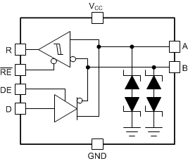
THVD24x9 devices are half-duplex RS-485 transceivers with integrated surge protection. Surge protection is achieved by integrating transient voltage suppressor (TVS) diodes in the standard 8-pin SOIC (D) package as well as small 10-pin VSON package. This feature increases the reliability by providing better immunity to noise transients coupled to the data cable which eliminates the need for external protection components.
THVD24x9 devices in the standard pin-out SOIC package operate from a single
3.3V or 5V supply. In addition, THVD24x9 devices in 10-pin VSON package and the V-versions of SOIC package support an additional VIO supply to operate the IOs from as low as 1.65V supply level. The devices in this family feature a wide common-mode voltage range making them suitable for multi-point applications over long cable runs.
| PART NUMBER | PACKAGE(1) | PACKAGE SIZE(2) |
|---|---|---|
| THVD2419, '2429 THVD2419V, '2429V | SOIC (8) | 4.9mm × 6mm |
| THVD2419, '2429 | VSON (10) | 3mm × 3mm |
 THVD24x9 Block Diagram (SOIC Package)
 THVD24x9 Block Diagram (VSON Package)