SLLSFP5 January 2024 THVD2419 , THVD2429
ADVANCE INFORMATION
- 1
- 1 Features
- 2 Applications
- 3 Description
- 4 Device Comparison Table
- 5 Pin Configuration and Functions
- 6 Specifications
- 7 Parameter Measurement Information
- 8 Detailed Description
- 9 Application and Implementation
- 10Device and Documentation Support
- 11Revision History
- 12Mechanical, Packaging, and Orderable Information
Package Options
Refer to the PDF data sheet for device specific package drawings
Mechanical Data (Package|Pins)
- DRC|10
Thermal pad, mechanical data (Package|Pins)
Orderable Information
12.1 Tape and Reel Information
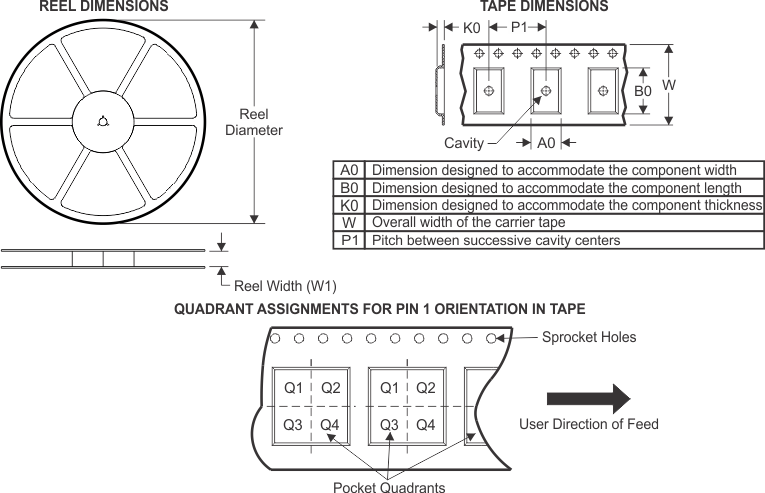
| Device | Package Type | Package Drawing | Pins | SPQ | Reel Diameter (mm) | Reel Width W1 (mm) | A0 (mm) | B0 (mm) | K0 (mm) | P1 (mm) | W (mm) | Pin1 Quadrant |
|---|---|---|---|---|---|---|---|---|---|---|---|---|
| PTHVD2419DR PTHVD2419VDR PTHVD2429DR PTHVD2429VDR | SOIC | D | 8 | 2500 | 330.0 | 12.4 | 6.4 | 5.2 | 2.1 | 8.0 | 12.0 | Q1 |
| PTHVD2419DRCR PTHVD2429DRCR | VSON | DRC | 10 | 5000 | 330.0 | 12.4 | 3.3 | 3.3 | 1.1 | 8.0 | 9.1 | Q2 |

| Device | Package Type | Package Drawing | Pins | SPQ | Length (mm) | Width (mm) | Height (mm) |
|---|---|---|---|---|---|---|---|
| PTHVD2419DR PTHVD2419VDR PTHVD2429DR PTHVD2429VDR |
SOIC | D | 8 | 2500 | 340.5 | 338.1 | 20.6 |
| PTHVD2419DRCR PTHVD2429DRCR |
VSON | DRC | 10 | 5000 | 367.0 | 367.0 | 35.0 |