SLLSF10 December 2019 TL16C750E
PRODUCTION DATA.
- 1 Features
- 2 Applications
- 3 Description
- 4 Revision History
- 5 Description (continued)
- 6 Pin Configuration and Functions
- 7 Specifications
- 8 Parameter Measurement Information
-
9 Detailed Description
- 9.1 Overview
- 9.2 Functional Block Diagrams
- 9.3
Feature Description
- 9.3.1 UART Modes
- 9.3.2 Trigger Levels
- 9.3.3 Hardware Flow Control
- 9.3.4 Auto-RTS
- 9.3.5 Auto-CTS
- 9.3.6 Software Flow Control
- 9.3.7 Software Flow Control Example
- 9.3.8 Reset
- 9.3.9 Interrupts
- 9.3.10 Interrupt Mode Operation
- 9.3.11 Polled Mode Operation
- 9.3.12 Break and Timeout Conditions
- 9.3.13 Programmable Baud Rate Generator with Fractional Divisor
- 9.3.14 Fractional Divisor
- 9.4 Device Functional Modes
- 9.5
Register Maps
- 9.5.1 Registers Operations
- 9.5.2 Receiver Holding Register (RHR)
- 9.5.3 Transmit Holding Register (THR)
- 9.5.4 FIFO Control Register (FCR)
- 9.5.5 Line Control Register (LCR)
- 9.5.6 Line Status Register (LSR)
- 9.5.7 Modem Control Register (MCR)
- 9.5.8 Modem Status Register (MSR)
- 9.5.9 Interrupt Enable Register (IER)
- 9.5.10 Interrupt Identification Register (IIR)
- 9.5.11 Enhanced Feature Register (EFR)
- 9.5.12 Divisor Latches (DLL, DLH, DLF)
- 9.5.13 Transmission Control Register (TCR)
- 9.5.14 Trigger Level Register (TLR)
- 9.5.15 FIFO Ready Register
- 9.5.16 Alternate Function Register (AFR)
- 9.5.17 RS-485 Mode
- 9.5.18 IrDA Overview
- 9.5.19 IrDA Encoder Function
- 10Application and Implementation
- 11Power Supply Recommendations
- 12Layout
- 13Device and Documentation Support
- 14Mechanical, Packaging, and Orderable Information
Package Options
Mechanical Data (Package|Pins)
- PFB|48
Thermal pad, mechanical data (Package|Pins)
- PFB|48
Orderable Information
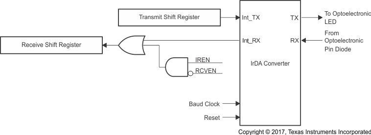
9.5.18 IrDA Overview
 Figure 34. IrDA Mode
 The IrDA defines several protocols for sending and receiving serial infrared data, including rates of 115.2 kbps, 0.576 Mbps, 1.152 Mbps, and 4 Mbps. The low rate of 115.2 kbps was specified first and the others must maintain downward compatibility with it. At the 115.2 kbps rate, the protocol implemented in the hardware is fairly simple. It primarily defines a serial infrared data word to be surrounded by a start bit equal to 0 and a stop bit equal to 1. Individual bits are encoded or decoded the same whether they are start, data, or stop bits. The IrDA engine in the TL16C750E device only evaluates single bits and follows the 115.2-kbps protocol. The 115.2-kbps rate is a maximum rate. When both ends of the transfer are setup to a lower but matching speed, the protocol still works. The clock used to code or sample the data is 16 times the baud rate, or 1.843-MHz maximum. To code a 1, no pulse is sent or received for 1-bit time period, or 16 clock cycles. To code a 0, one pulse is sent or received within a 1-bit time period, or 16 clock cycles. The pulse must be at least 1.6-μs wide and 3 clock cycles long at 1.843 MHz. At lower baud rates the pulse can be 1.6 μs wide or as long as 3 clock cycles. The transmitter output, TX, is intended to drive a LED circuit to generate an infrared pulse. The LED circuits work on positive pulses. A terminal circuit is expected to create the receiver input, RX. Most, but not all, PIN circuits have inversion and generate negative pulses from the detected infrared light. Their output is normally high. The TL16C750E device can decode either negative or positive pulses on RX.