SLLSF10 December 2019 TL16C750E
PRODUCTION DATA.
- 1 Features
- 2 Applications
- 3 Description
- 4 Revision History
- 5 Description (continued)
- 6 Pin Configuration and Functions
- 7 Specifications
- 8 Parameter Measurement Information
-
9 Detailed Description
- 9.1 Overview
- 9.2 Functional Block Diagrams
- 9.3
Feature Description
- 9.3.1 UART Modes
- 9.3.2 Trigger Levels
- 9.3.3 Hardware Flow Control
- 9.3.4 Auto-RTS
- 9.3.5 Auto-CTS
- 9.3.6 Software Flow Control
- 9.3.7 Software Flow Control Example
- 9.3.8 Reset
- 9.3.9 Interrupts
- 9.3.10 Interrupt Mode Operation
- 9.3.11 Polled Mode Operation
- 9.3.12 Break and Timeout Conditions
- 9.3.13 Programmable Baud Rate Generator with Fractional Divisor
- 9.3.14 Fractional Divisor
- 9.4 Device Functional Modes
- 9.5
Register Maps
- 9.5.1 Registers Operations
- 9.5.2 Receiver Holding Register (RHR)
- 9.5.3 Transmit Holding Register (THR)
- 9.5.4 FIFO Control Register (FCR)
- 9.5.5 Line Control Register (LCR)
- 9.5.6 Line Status Register (LSR)
- 9.5.7 Modem Control Register (MCR)
- 9.5.8 Modem Status Register (MSR)
- 9.5.9 Interrupt Enable Register (IER)
- 9.5.10 Interrupt Identification Register (IIR)
- 9.5.11 Enhanced Feature Register (EFR)
- 9.5.12 Divisor Latches (DLL, DLH, DLF)
- 9.5.13 Transmission Control Register (TCR)
- 9.5.14 Trigger Level Register (TLR)
- 9.5.15 FIFO Ready Register
- 9.5.16 Alternate Function Register (AFR)
- 9.5.17 RS-485 Mode
- 9.5.18 IrDA Overview
- 9.5.19 IrDA Encoder Function
- 10Application and Implementation
- 11Power Supply Recommendations
- 12Layout
- 13Device and Documentation Support
- 14Mechanical, Packaging, and Orderable Information
Package Options
Mechanical Data (Package|Pins)
- PFB|48
Thermal pad, mechanical data (Package|Pins)
- PFB|48
Orderable Information
11 Power Supply Recommendations
The power supply must provide a constant voltage with a 10% maximum variation of the nominal value and has to be able to provide at least the maximum current consumption of the device for the selected nominal voltage only for the UART device:
- VCC = 1.8 V
- VCC = 2.5 V
- VCC = 3.3 V
- VCC = 5 V
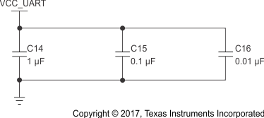
The VCC pin must have a 1-µF bypass capacitor placed as close as possible to this pin. Also, TI recommends to include two extra capacitors in parallel, which should also be placed as close as possible to the VCC pin. The suggested values for these extra capacitors are 0.1 µF and 0.01 µF, respectively.

Place as close as possible to the VCC pin of the UART.
Figure 45. Recommended Bypass Capacitors Array