SLLSF10 December 2019 TL16C750E
PRODUCTION DATA.
- 1 Features
- 2 Applications
- 3 Description
- 4 Revision History
- 5 Description (continued)
- 6 Pin Configuration and Functions
- 7 Specifications
- 8 Parameter Measurement Information
-
9 Detailed Description
- 9.1 Overview
- 9.2 Functional Block Diagrams
- 9.3
Feature Description
- 9.3.1 UART Modes
- 9.3.2 Trigger Levels
- 9.3.3 Hardware Flow Control
- 9.3.4 Auto-RTS
- 9.3.5 Auto-CTS
- 9.3.6 Software Flow Control
- 9.3.7 Software Flow Control Example
- 9.3.8 Reset
- 9.3.9 Interrupts
- 9.3.10 Interrupt Mode Operation
- 9.3.11 Polled Mode Operation
- 9.3.12 Break and Timeout Conditions
- 9.3.13 Programmable Baud Rate Generator with Fractional Divisor
- 9.3.14 Fractional Divisor
- 9.4 Device Functional Modes
- 9.5
Register Maps
- 9.5.1 Registers Operations
- 9.5.2 Receiver Holding Register (RHR)
- 9.5.3 Transmit Holding Register (THR)
- 9.5.4 FIFO Control Register (FCR)
- 9.5.5 Line Control Register (LCR)
- 9.5.6 Line Status Register (LSR)
- 9.5.7 Modem Control Register (MCR)
- 9.5.8 Modem Status Register (MSR)
- 9.5.9 Interrupt Enable Register (IER)
- 9.5.10 Interrupt Identification Register (IIR)
- 9.5.11 Enhanced Feature Register (EFR)
- 9.5.12 Divisor Latches (DLL, DLH, DLF)
- 9.5.13 Transmission Control Register (TCR)
- 9.5.14 Trigger Level Register (TLR)
- 9.5.15 FIFO Ready Register
- 9.5.16 Alternate Function Register (AFR)
- 9.5.17 RS-485 Mode
- 9.5.18 IrDA Overview
- 9.5.19 IrDA Encoder Function
- 10Application and Implementation
- 11Power Supply Recommendations
- 12Layout
- 13Device and Documentation Support
- 14Mechanical, Packaging, and Orderable Information
Package Options
Mechanical Data (Package|Pins)
- PFB|48
Thermal pad, mechanical data (Package|Pins)
- PFB|48
Orderable Information
9.5.17 RS-485 Mode
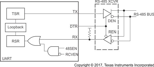
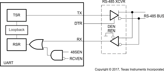
The RS-485 mode is intended to simplify the interface between the UART and an RS-485 driver or transceiver. When enabled by setting 485EN, the DTR output goes high one bit time before the first stop bit of the first data byte being sent, and remains high as long as there is pending data in the TSR or THR (xmt fifo). After both are empty (after the last stop bit of the last data byte), the DTR output stays high for a programmable delay of 0 to 15 bit times, as set by DLY[2:0]. This helps preserve data integrity over long signal lines. This is illustrated in the following.
Often RS-485 packets are relatively short and the entire packet can fit within the 128 byte xmt fifo. In this case, it goes empty when the TSR goes empty. But in cases where a larger block needs to be sent, it is advantageous to reload the xmt fifo as soon as it is depleted. Otherwise, the transmission stalls while waiting for the xmt fifo to be reloaded, which varies with processor load. In this case, it is best to also set 485LG (large block), which causes the transmit interrupt to occur wither when the THR becomes empty (if the xmt fifo level was not above the threshold), or when the xmt fifo threshold is crossed. The reloading of the xmt fifo occurs while some data is being shifted out, eliminating fifo underrun. If desired, when the last bytes of a current transmission are being loaded in the xmt fifo, 485LG can be cleared before the load and the transmit interrupt occurs on the TSR going empty.

 Figure 32. RS-485 Application Example 1
  Figure 33. RS-485 Application Example 2