SGLS007G February 2003 – August 2022 TLC2272-Q1 , TLC2272A-Q1 , TLC2274-Q1 , TLC2274A-Q1
PRODUCTION DATA
- 1 Features
- 2 Applications
- 3 Description
- 4 Revision History
- 5 Pin Configuration and Functions
-
6 Specifications
- 6.1 Absolute Maximum Ratings
- 6.2 ESD Ratings
- 6.3 Recommended Operating Conditions
- 6.4 Thermal Information
- 6.5 Electrical Characteristics: VDD = 5 V (TLC2272-Q1 and TLC2272A-Q1)
- 6.6 Electrical Characteristics: VDD± = ±5 V (TLC2272-Q1 and TLC2272A-Q1)
- 6.7 Electrical Characteristics: VDD = 5 V (TLC2274-Q1 and TLC2274A-Q1)
- 6.8 Electrical Characteristics: VDD± = ±5 V (TLC2274-Q1 and TLC2274A-Q1)
- 6.9 Typical Characteristics
- 7 Detailed Description
- 8 Application and Implementation
- 9 Device and Documentation Support
- 10Mechanical, Packaging, and Orderable Information
Package Options
Mechanical Data (Package|Pins)
Thermal pad, mechanical data (Package|Pins)
Orderable Information
8.2.2.1 Differential Amplifier Equations
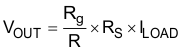
Equation 1 and Equation 2 are used to calculate VOUT.
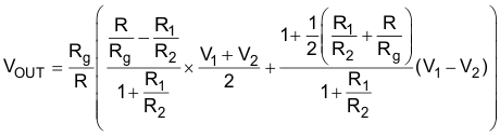
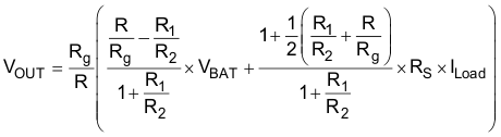
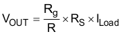
In an ideal case, Equation 3 then calculates R1 = R and R2 = Rg, and VOUT:
However, the resistors have tolerances; therefore, the resistors cannot be perfectly matched.
R1 = R ± ΔR1
R2 = R2 ± ΔR2
R = R ± ΔR
Rg = Rg ± ΔRg

Equation 5 shows that by developing the equations and neglecting the second order, the worst case is when the tolerances add up:
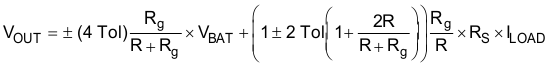
where
- Tol = 0.01 for 1%
- Tol = 0.001 for 0.1%
If the resistors are perfectly matched, then Tol = 0 and Equation 6 calculates VOUT:
The highest error is from the common mode:
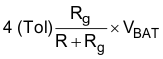
Gain of 10, Rg / R = 10, and Tol = 1%:
Common mode error = ((4 × 0.01) / 1.1) × 12 V = 0.436 V
Gain of 10 and Tol = 0.1%:
Common mode error = 43.6 mV
The resistors were chosen from 2% batches.
R1 and R 12 kΩ
R2 and Rg 120 kΩ
Ideal Gain = 120 / 12 = 10
The measured value of the resistors:
R1 = 11.835 kΩ
R = 11.85 kΩ
R2 = 117.92 kΩ
Rg = 118.07 kΩ