SGLS007G February 2003 – August 2022 TLC2272-Q1 , TLC2272A-Q1 , TLC2274-Q1 , TLC2274A-Q1
PRODUCTION DATA
- 1 Features
- 2 Applications
- 3 Description
- 4 Revision History
- 5 Pin Configuration and Functions
-
6 Specifications
- 6.1 Absolute Maximum Ratings
- 6.2 ESD Ratings
- 6.3 Recommended Operating Conditions
- 6.4 Thermal Information
- 6.5 Electrical Characteristics: VDD = 5 V (TLC2272-Q1 and TLC2272A-Q1)
- 6.6 Electrical Characteristics: VDD± = ±5 V (TLC2272-Q1 and TLC2272A-Q1)
- 6.7 Electrical Characteristics: VDD = 5 V (TLC2274-Q1 and TLC2274A-Q1)
- 6.8 Electrical Characteristics: VDD± = ±5 V (TLC2274-Q1 and TLC2274A-Q1)
- 6.9 Typical Characteristics
- 7 Detailed Description
- 8 Application and Implementation
- 9 Device and Documentation Support
- 10Mechanical, Packaging, and Orderable Information
Package Options
Mechanical Data (Package|Pins)
Thermal pad, mechanical data (Package|Pins)
Orderable Information
3 Description
The TLC227x-Q1 are dual and quad, LinCMOS™ operational amplifiers. Both devices exhibit rail-to-rail output performance for increased dynamic range in single- or split-supply applications. The TLC227x-Q1 family offers 2 MHz of bandwidth and 3 V/μs of slew rate for higher-speed applications. These devices offer comparable ac performance while having better noise, input offset voltage, and power dissipation than existing CMOS op amps. The TLC227x‑Q1 has a noise voltage of 9 nV/√Hz—two times lower than competitive solutions.
The TLC227x-Q1, exhibiting high input impedance and low noise, are excellent for small-signal conditioning for high-impedance sources, such as piezoelectric transducers. In addition, the rail-to-rail output feature, with single- or split-supplies, makes this family a great choice when interfacing with analog-to-digital converters (ADCs).
For precision applications, the TLC227xA-Q1 family is available with a maximum input offset voltage of 950 μV. This family is fully characterized at 5 V and ±5 V.
These devices offer increased output dynamic range, lower noise voltage, and lower input offset voltage. This enhanced feature set allows the TLC227x-Q1 to be used in a wider range of applications. For applications that require higher output drive and wider input voltage range, see the TLV2432-Q1 and TLV2442-Q1. All the parameters of the TLC227x-Q1 family enables these devices to be applicable in most automotive applications.
| PART NUMBER | PACKAGE(1) | BODY SIZE (NOM) |
|---|---|---|
| TLC2272-Q1, TLC2272A-Q1 | SOIC (8) | 4.90 mm x 3.91 mm |
| TSSOP (8) | 3.00 mm × 4.40 mm | |
| TLC2274-Q1, TLC2274A-Q1 | SOIC (14) | 8.65 mm x 3.91 mm |
| TSSOP (14) | 5.00 mm × 4.40 mm |
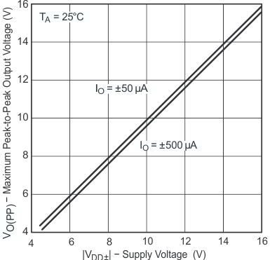
 Maximum Peak-To-Peak Output Voltage vs Supply Voltage