SGLS008G March 2003 – February 2018 TLV2460A-Q1 , TLV2461A-Q1 , TLV2462-Q1 , TLV2462A-Q1 , TLV2463A-Q1 , TLV2464A-Q1
PRODUCTION DATA.
- 1 Features
- 2 Applications
- 3 Description
- 4 Revision History
- 5 Pin Configuration and Functions
-
6 Specifications
- 6.1 Absolute Maximum Ratings
- 6.2 ESD Ratings
- 6.3 Recommended Operating Conditions
- 6.4 Thermal Information: TLV2460x-Q1
- 6.5 Thermal Information: TLV2461x-Q1
- 6.6 Thermal Information: TLV2462-Q1
- 6.7 Thermal Information: TLV2462A-Q1
- 6.8 Thermal Information: TLV2463x-Q1
- 6.9 Electrical Characteristics: VDD = 3 V
- 6.10 Electrical Characteristics: VDD = 5 V
- 6.11 Operating Characteristics: VDD = 3 V
- 6.12 Operating Characteristics: VDD = 5 V
- 6.13 Typical Characteristics
- 7 Parameter Measurement Information
- 8 Detailed Description
- 9 Application and Implementation
- 10Power Supply Recommendations
- 11Layout
- 12Device and Documentation Support
- 13Mechanical, Packaging, and Orderable Information
Package Options
Refer to the PDF data sheet for device specific package drawings
Mechanical Data (Package|Pins)
- PW|14
Thermal pad, mechanical data (Package|Pins)
Orderable Information
9.2.2 Detailed Design Procedure
The following section shows the detailed design procedure. See Equation 2 for the type-3 compensation gain.

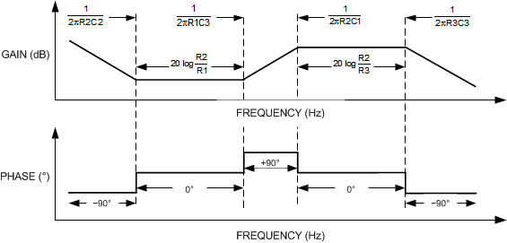
Type-3 compensation poles and zeros are shown in the preferred asymptotic graph; see Figure 56. Relocate the compensation poles and zeroes by changing the values of the resistors and capacitors according to the compensation requirement. The operational amplifier cannot achieve the preferred case because of the open-loop gain and phase limitation of the amplifier.
 Figure 56. Preferred Asymptotic Graph
The poles and zeros are calculated assuming C2 >> C1 and R1 >> R3. This assumption is correct because the C1 and R3 components set the high frequencies.
This TLV226x-Q1 device type-3 compensation circuit design boosts the gain and phase for the DC-to-DC converter around 30-KHz resonance frequencies. This corresponds to 1 µH and 22 µF for the output filter.
The operational amplifier is configured as type-2 compensation by omitting the C3 capacitor. Type-2 compensates the DC-to-DC converter with an output capacitor with a series resistor ESR; see Equation 3.
