SGLS008G March 2003 – February 2018 TLV2460A-Q1 , TLV2461A-Q1 , TLV2462-Q1 , TLV2462A-Q1 , TLV2463A-Q1 , TLV2464A-Q1
PRODUCTION DATA.
- 1 Features
- 2 Applications
- 3 Description
- 4 Revision History
- 5 Pin Configuration and Functions
-
6 Specifications
- 6.1 Absolute Maximum Ratings
- 6.2 ESD Ratings
- 6.3 Recommended Operating Conditions
- 6.4 Thermal Information: TLV2460x-Q1
- 6.5 Thermal Information: TLV2461x-Q1
- 6.6 Thermal Information: TLV2462-Q1
- 6.7 Thermal Information: TLV2462A-Q1
- 6.8 Thermal Information: TLV2463x-Q1
- 6.9 Electrical Characteristics: VDD = 3 V
- 6.10 Electrical Characteristics: VDD = 5 V
- 6.11 Operating Characteristics: VDD = 3 V
- 6.12 Operating Characteristics: VDD = 5 V
- 6.13 Typical Characteristics
- 7 Parameter Measurement Information
- 8 Detailed Description
- 9 Application and Implementation
- 10Power Supply Recommendations
- 11Layout
- 12Device and Documentation Support
- 13Mechanical, Packaging, and Orderable Information
Package Options
Refer to the PDF data sheet for device specific package drawings
Mechanical Data (Package|Pins)
- PW|14
Thermal pad, mechanical data (Package|Pins)
Orderable Information
8.3.3 General Configurations
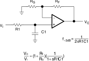
When receiving low-level signals, limiting the bandwidth of the incoming signals into the system is often required. To limit bandwidth, place an RC filter at the noninverting terminal of the amplifier (see Figure 51).
 Figure 51. Single-Pole Low-Pass Filter
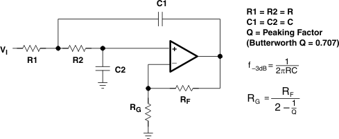
If even more attenuation is required, a multiple pole filter is required. Use a Sallen-Key filter for this task; see Figure 52. For best results, the amplifier must have a bandwidth that is eight to ten times the filter frequency bandwidth. Failure to do this can result in phase shift of the amplifier.
 Figure 52. 2-Pole Low-Pass Sallen-Key Filter