SLAS509G April 2006 – July 2021 TLV320AIC3106
PRODUCTION DATA
- 1 Features
- 2 Applications
- 3 Description
- 4 Revision History
- 5 Description (continued)
- 6 Device Comparison Table
- 7 Pin Configuration and Functions
- 8 Specifications
- 9 Parameter Measurement Information
-
10Detailed Description
- 10.1 Overview
- 10.2 Functional Block Diagram
- 10.3
Feature Description
- 10.3.1 Hardware Reset
- 10.3.2 Digital Audio Data Serial Interface
- 10.3.3 Audio Data Converters
- 10.3.4 Audio Analog Inputs
- 10.3.5 Analog Fully Differential Line Output Drivers
- 10.3.6 Analog High Power Output Drivers
- 10.3.7 Input Impedance and VCM Control
- 10.3.8 General-Purpose I/O
- 10.3.9 Digital Microphone Connectivity
- 10.3.10 Micbias Generation
- 10.3.11 Short Circuit Output Protection
- 10.3.12 Jack/Headset Detection
- 10.4 Device Functional Modes
- 10.5 Programming
- 10.6 Register Maps
- 11Application and Implementation
- 12Power Supply Recommendations
- 13Layout
- 14Device and Documentation Support
Package Options
Mechanical Data (Package|Pins)
Thermal pad, mechanical data (Package|Pins)
- RGZ|48
Orderable Information
10.4.1.3 Passive Analog Bypass During Powerdown
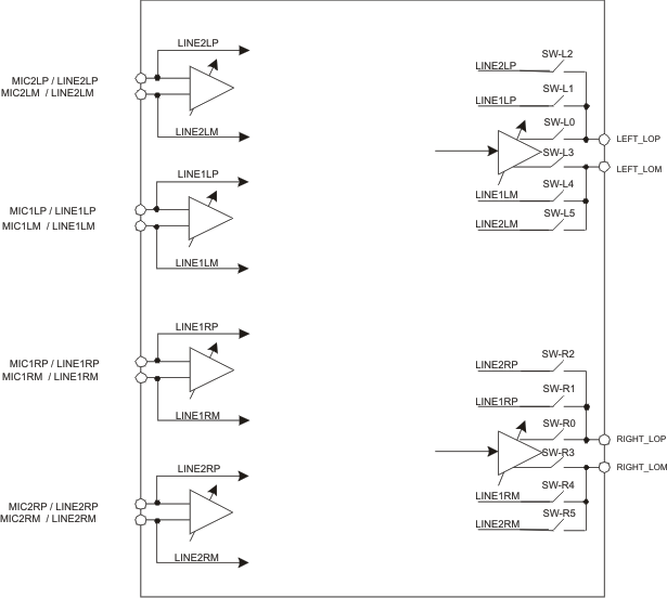
Programming the TLV320AIC3106 to Passive Analog bypass occurs by configuring the output stage switches for pass through. This is done by opening switches SW-L0, SW-L3, SW-R0, SW-R3 and closing either SW-L1 or SW-L2 and SW-R1 or SW-R2. See Figure 10-20 Passive Analog Bypass Mode Configuration. Programming this mode is done by writing to Page 0, Register 108.
Connecting MIC1LP/LINE1LP input signal to the LEFT_LOP pin is done by closing SW-L1 and opening SW-L0, this action is done by writing a “1” to Page 0, Register 108, Bit D0. Connecting MIC2LP/LINE2LP input signal to the LEFT_LOP pin is done by closing SW-L2 and opening SW-L0, this action is done by writing a “1” to Page 0, Register 108, Bit D2. Connecting MIC1LM/LINE1LM input signal to the LEFT_LOM pin is done by closing SW-L4 and opening SW-L3, this action is done by writing a “1” to Page 0, Register 108, Bit D1. Connecting MIC2LM/LINE2LM input signal to the LEFT_LOM pin is done by closing SW-L5 and opening SW-L3, this action is done by writing a “1” to Page 0, Register 108, Bit D3.
Connecting MIC1RP/LINE1RP input signal to the RIGHT_LOP pin is done by closing SW-R1 and opening SW-R0, this action is done by writing a “1” to Page 0, Register 108, Bit D4. Connecting MIC2RP/LINE2RP input signal to the RIGHT_LOP pin is done by closing SW-R2 and opening SW-R0, this action is done by writing a “1” to Page 0, Register 108, Bit D6. Connecting MIC1RM/LINE1RM input signal to the RIGHT_LOM pin is done by closing SW-R4 and opening SW-R3, this action is done by writing a “1” to Page 0, Register 108, Bit D5. Connecting MIC2RM/LINE2RM input signal to the RIGHT_LOM pin is done by closing SW-R5 and opening SW-R3, this action is done by writing a “1” to Page 0, Register 108, Bit D7. A diagram of the passive analog bypass mode configuration can be seen in Figure 10-20.
In general, connecting two switches to the same output pin should be avoided, as this error will short two input signals together, and would like cause distortion of the signal as the two signal are in contention, and poor frequency response would also likely occur.
 Figure 10-20 Passive Analog Bypass Mode Configuration