SLAS509G April 2006 – July 2021 TLV320AIC3106
PRODUCTION DATA
- 1 Features
- 2 Applications
- 3 Description
- 4 Revision History
- 5 Description (continued)
- 6 Device Comparison Table
- 7 Pin Configuration and Functions
- 8 Specifications
- 9 Parameter Measurement Information
-
10Detailed Description
- 10.1 Overview
- 10.2 Functional Block Diagram
- 10.3
Feature Description
- 10.3.1 Hardware Reset
- 10.3.2 Digital Audio Data Serial Interface
- 10.3.3 Audio Data Converters
- 10.3.4 Audio Analog Inputs
- 10.3.5 Analog Fully Differential Line Output Drivers
- 10.3.6 Analog High Power Output Drivers
- 10.3.7 Input Impedance and VCM Control
- 10.3.8 General-Purpose I/O
- 10.3.9 Digital Microphone Connectivity
- 10.3.10 Micbias Generation
- 10.3.11 Short Circuit Output Protection
- 10.3.12 Jack/Headset Detection
- 10.4 Device Functional Modes
- 10.5 Programming
- 10.6 Register Maps
- 11Application and Implementation
- 12Power Supply Recommendations
- 13Layout
- 14Device and Documentation Support
Package Options
Mechanical Data (Package|Pins)
Thermal pad, mechanical data (Package|Pins)
- RGZ|48
Orderable Information
10.3.5 Analog Fully Differential Line Output Drivers
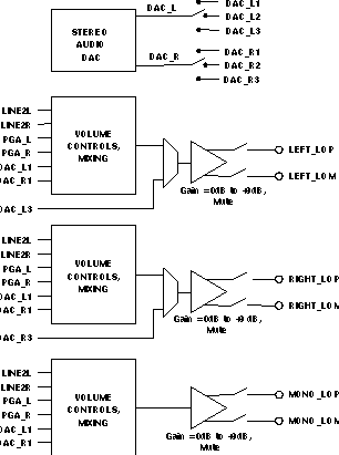
The TLV320AIC3106 has two fully differential line output drivers, each capable of driving a 10-kΩ differential load. The output stage design leading to the fully differential line output drivers is shown in Figure 10-14 and Figure 10-15. This design includes extensive capability to adjust signal levels independently before any mixing occurs, beyond that already provided by the PGA gain and the DAC digital volume control.
 Figure 10-14 Architecture of the Output Stage Leading to the Fully Differential Line Output Drivers
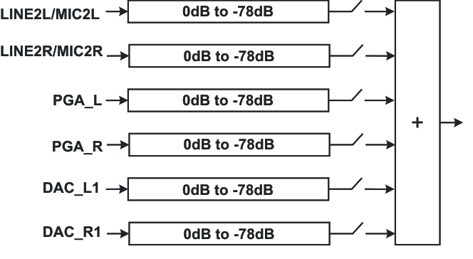
The LINE2L/R signals refer to the signals that travel through the analog input bypass path to the output stage. The PGA_L/R signals refer to the outputs of the ADC PGA stages that are similarly passed around the ADC to the output stage. Note that since both left and right channel signals are routed to all output drivers, a mono mix of any of the stereo signals can easily be obtained by setting the volume controls of both left and right channel signals to –6 dB and mixing them. Undesired signals can also be disconnected from the mix as well through register control.
 Figure 10-15 Detail of the Volume Control and Mixing Function Shown in Figure 10-10 and Figure 10-25
The DAC_L/R signals are the outputs of the stereo audio DAC, which can be steered by register control based on the requirements of the system. If mixing of the DAC audio with other signals is not required, and the DAC output is only needed at the stereo line outputs, then it is recommended to use the routing through path DAC_L3/R3 to the fully differential stereo line outputs. This results not only in higher quality output performance, but also in lower power operation, since the analog volume controls and mixing blocks ahead of these drivers can be powered down.
If instead the DAC analog output must be routed to multiple output drivers simultaneously (such as to LEFT_LOP/M, RIGHT_LOP/M, and MONO_LOP/M) or must be mixed with other analog signals, then the DAC outputs should be switched through the DAC_L1/R1 path. This option provides the maximum flexibility for routing of the DAC analog signals to the output drivers
The TLV320AIC3106 includes an output level control on each output driver with limited gain adjustment from 0 dB to 9 dB. The output driver circuitry in this device are designed to provide a low distortion output while playing fullscale stereo DAC signals at a 0dB gain setting. However, a higher amplitude output can be obtained at the cost of increased signal distortion at the output. This output level control allows the user to make this tradeoff based on the requirements of the end equipment. Note that this output level control is not intended to be used as a standard output volume control. It is expected to be used only sparingly for level setting, that is, adjustment of the fullscale output range of the device.
The PGA_L/R signals refer to the outputs of the ADC PGA stages that are similarly passed around the ADC to the output stage. Note that because both left- and right-channel signals are routed to all output drivers, a mono mix of any of the stereo signals can easily be obtained by setting the volume controls of both left- and right-channel signals to –6 dB and mixing them. Undesired signals can also be disconnected from the mix as well through register control.