SLAS509G April   2006  – July 2021 TLV320AIC3106

PRODUCTION DATA  

  1. Features
  2. Applications
  3. Description
  4. Revision History
  5. Description (continued)
  6. Device Comparison Table
  7. Pin Configuration and Functions
  8. Specifications
    1. 8.1 Absolute Maximum Ratings
    2. 8.2 ESD Ratings
    3. 8.3 Recommended Operating Conditions
    4. 8.4 Thermal Information
    5. 8.5 Electrical Characteristics
    6. 8.6 Timing Requirements: Audio Data Serial Interface (1)
    7. 8.7 Timing Diagrams
    8. 8.8 Typical Characteristics
  9. Parameter Measurement Information
  10. 10Detailed Description
    1. 10.1 Overview
    2. 10.2 Functional Block Diagram
    3. 10.3 Feature Description
      1. 10.3.1  Hardware Reset
      2. 10.3.2  Digital Audio Data Serial Interface
        1. 10.3.2.1 Right-Justified Mode
        2. 10.3.2.2 Left-Justified Mode
        3. 10.3.2.3 I2S Mode
        4. 10.3.2.4 DSP Mode
        5. 10.3.2.5 TDM Data Transfer
      3. 10.3.3  Audio Data Converters
        1. 10.3.3.1 Audio Clock Generation
        2. 10.3.3.2 Stereo Audio ADC
          1. 10.3.3.2.1 Stereo Audio ADC High-Pass Filter
          2. 10.3.3.2.2 Automatic Gain Control (AGC)
            1. 10.3.3.2.2.1 Target Level
            2. 10.3.3.2.2.2 Attack Time
            3. 10.3.3.2.2.3 Decay Time
            4. 10.3.3.2.2.4 Noise Gate Threshold
            5. 10.3.3.2.2.5 Maximum PGA Gain Applicable
        3. 10.3.3.3 Stereo Audio DAC
          1. 10.3.3.3.1 Digital Audio Processing for Playback
          2. 10.3.3.3.2 Digital Interpolation Filter
          3. 10.3.3.3.3 Delta-Sigma Audio DAC
          4. 10.3.3.3.4 Audio DAC Digital Volume Control
          5. 10.3.3.3.5 Increasing DAC Dynamic Range
          6. 10.3.3.3.6 Analog Output Common-Mode Adjustment
          7. 10.3.3.3.7 Audio DAC Power Control
      4. 10.3.4  Audio Analog Inputs
      5. 10.3.5  Analog Fully Differential Line Output Drivers
      6. 10.3.6  Analog High Power Output Drivers
      7. 10.3.7  Input Impedance and VCM Control
      8. 10.3.8  General-Purpose I/O
      9. 10.3.9  Digital Microphone Connectivity
      10. 10.3.10 Micbias Generation
      11. 10.3.11 Short Circuit Output Protection
      12. 10.3.12 Jack/Headset Detection
    4. 10.4 Device Functional Modes
      1. 10.4.1 Bypass Path Mode
        1. 10.4.1.1 Analog Input Bypass Path Functionality
        2. 10.4.1.2 ADC PGA Signal Bypass Path Functionality
        3. 10.4.1.3 Passive Analog Bypass During Powerdown
      2. 10.4.2 Digital Audio Processing for Record Path
    5. 10.5 Programming
      1. 10.5.1 Digital Control Serial Interface
        1. 10.5.1.1 SPI Control Mode
          1. 10.5.1.1.1 SPI Communication Protocol
          2. 10.5.1.1.2 Limitation on Register Writing
          3. 10.5.1.1.3 Continuous Read / Write Operation
        2. 10.5.1.2 I2C Control Interface
          1. 10.5.1.2.1 I2C BUS Debug in a Glitched System
    6. 10.6 Register Maps
      1. 10.6.1 Output Stage Volume Controls
  11. 11Application and Implementation
    1. 11.1 Application Information
    2. 11.2 Typical Application
      1. 11.2.1 Design Requirements
      2. 11.2.2 Detailed Design Procedure
      3. 11.2.3 Application Curves
  12. 12Power Supply Recommendations
  13. 13Layout
    1. 13.1 Layout Guidelines
    2. 13.2 Layout Examples
  14. 14Device and Documentation Support
    1. 14.1 Receiving Notification of Documentation Updates
    2. 14.2 Support Resources
    3. 14.3 Trademarks
    4. 14.4 Electrostatic Discharge Caution
    5. 14.5 Glossary

Package Options

Mechanical Data (Package|Pins)
Thermal pad, mechanical data (Package|Pins)
Orderable Information

Digital Audio Processing for Record Path

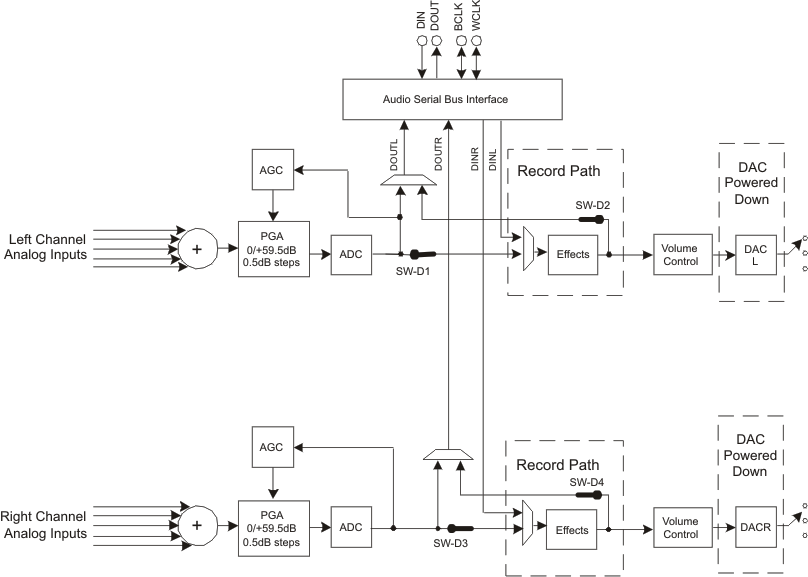
In applications where record only is selected, and DAC is powered down, the playback path signal processing blocks can be used in the ADC record path. These filtering blocks can support high pass, low pass, band pass or notch filtering. In this mode, the record only path has switches SW-D1 through SW-D4 closed, and reroutes the ADC output data through the digital signal processing blocks. Since the DAC's Digital Signal Processing blocks are being re-used, naturally the addresses of these digital filter coefficients are the same as for the DAC digital processing and are located on Page 1, Registers 1-52. This record only mode is enabled by powering down both DACs by writing to Page 0, Register 37, bits D7-D6 (D7=D6=”0”). Next, enable the digital filter pathway for the ADC by writing a “1” to Page 0, Register 107, bit D3. (Note, this pathway is only enabled if both DACs are powered down.) This record only path can be seen in Figure 10-21.
GUID-A811A8F9-5831-47A3-8CF4-585EACE13D41-low.gifFigure 10-21 Record Only Mode With Digital Processing Path Enabled