SNOSDA2E august 2020 – july 2023 TLV3604 , TLV3605 , TLV3607
PRODMIX
- 1
- 1 Features
- 2 Applications
- 3 Description
- 4 Revision History
- 5 Pin Configuration and Functions
- 6 Specifications
- 7 Detailed Description
- 8 Application and Implementation
- 9 Power Supply Recommendations
- 10Layout
- 11Device and Documentation Support
- 12Mechanical, Packaging, and Orderable Information
Package Options
Mechanical Data (Package|Pins)
- RVK|12
Thermal pad, mechanical data (Package|Pins)
Orderable Information
3 Description
The TLV3604, TLV3605 (single channel), and TLV3607 (dual channel) are 800-ps, high-speed comparators with LVDS outputs and rail-to-rail inputs. These features, along with an operating voltage range of 2.4 V to 5.5 V and a high toggle frequency of 3 Gbps, make them well suited for LIDAR, clock and data recovery applications, and test and measurement systems.
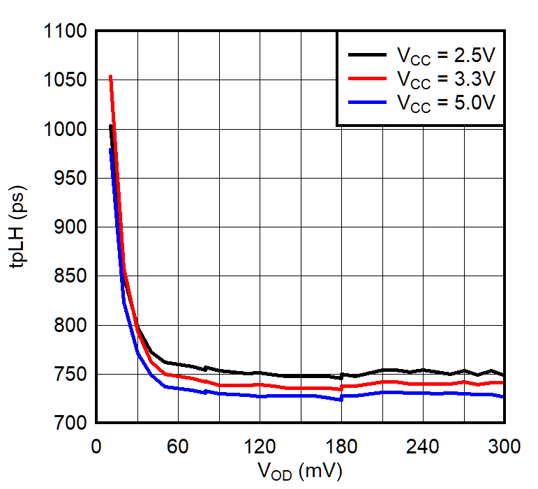
Likewise, the TLV3604, TLV3605 and TLV3607 have strong input overdrive performance of 350 ps and are able to detect narrow pulse widths of just 600 ps. This combination of low variation in propagation delay due to input overdrive and the ability to detect narrow pulses improve system performance and extend distance range in Time-of-Flight (ToF) applications.
The Low-Voltage-Differential-Signal (LVDS) output of the TLV3604, TLV3605, and TLV3607 also helps increase data throughput and optimizes power consumption. The complementary outputs reduce EMI by suppressing common mode noise on each output. The LVDS output is designed to drive and interface directly with downstream devices that accept a standard LVDS input, such as high-speed FPGAs and CPUs.
The TLV3604 is in a tiny 6 pin SC-70 package, which makes it easier for space sensitive applications such as an optical sensor module. The TLV3605 (single) and TLV3607 (dual) maintain the same performance as the TLV3604, and offer adjustable hysteresis control, shutdown, and latching features in 12 pin QFN and 16 pin WQFN packages, making them excellent choices for test and measurement applications.
| PART NUMBER | PACKAGE (1) | BODY SIZE (NOM) |
|---|---|---|
| TLV3604 | SC70 (6) | 1.25 mm × 2.00 mm |
| TLV3605 | QFN (12) | 3.00 mm × 3.00 mm |
| TLV3607 | WQFN (16) | 4.00 mm × 4.00 mm |
1. For all orderable packages, see the orderable addendum at the end of the datasheet.
 TpLH v. Overdrive Dispersion
 Functional Block Diagram