SBOS833R October 2017 – November 2021 TLV9001 , TLV9002 , TLV9004
PRODUCTION DATA
- 1
- 1 Features
- 2 Applications
- 3 Description
- 4 Revision History
- 5 Device Comparison Table
- 6 Pin Configuration and Functions
-
7 Specifications
- 7.1 Absolute Maximum Ratings
- 7.2 ESD Ratings
- 7.3 Recommended Operating Conditions
- 7.4 Thermal Information: TLV9001
- 7.5 Thermal Information: TLV9001S
- 7.6 Thermal Information: TLV9002
- 7.7 Thermal Information: TLV9002S
- 7.8 Thermal Information: TLV9004
- 7.9 Thermal Information: TLV9004S
- 7.10 Electrical Characteristics
- 7.11 Typical Characteristics
- 8 Detailed Description
- 9 Application and Implementation
- 10Power Supply Recommendations
- 11Layout
- 12Device and Documentation Support
- 13Mechanical, Packaging, and Orderable Information
Package Options
Mechanical Data (Package|Pins)
Thermal pad, mechanical data (Package|Pins)
Orderable Information
9.2.2.2 Detailed Design Procedure
The transfer function between the output voltage (VOUT), the input current, (IIN) and the reference voltage (VREF) is defined in Equation 5.

Where:
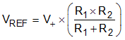
Set VREF to 100 mV to meet the minimum output voltage level by setting R1 and R2 to meet the required ratio calculated in Equation 7.
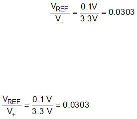
The closest resistor ratio to meet this ratio sets R1 to 11.5 kΩ and R2 to 357 Ω.
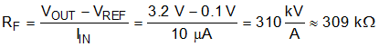
The required feedback resistance can be calculated based on the input current and desired output voltage.
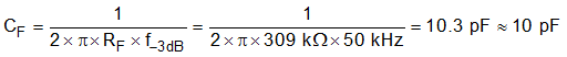
Calculate the value for the feedback capacitor based on RF and the desired –3-dB bandwidth, (f–3dB) using Equation 9.
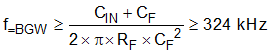
The minimum op amp bandwidth required for this application is based on the value of RF, CF, and the capacitance on the INx– pin of the TLV9002 which is equal to the sum of the photodiode shunt capacitance, (CPD) the common-mode input capacitance, (CCM) and the differential input capacitance (CD) as Equation 10 shows.

The minimum op amp bandwidth is calculated in Equation 11.
The 1-MHz bandwidth of the TLV900x meets the minimum bandwidth requirement and remains stable in this application configuration.