SBOSA71 July 2021 TMCS1107-Q1
PRODUCTION DATA
- 1 Features
- 2 Applications
- 3 Description
- 4 Revision History
- 5 Device Comparison
- 6 Pin Configuration and Functions
- 7 Specifications
- 8 Parameter Measurement Information
- 9 Detailed Description
- 10Application and Implementation
- 11Power Supply Recommendations
- 12Layout
- 13Device and Documentation Support
- 14Mechanical, Packaging, and Orderable Information
Package Options
Refer to the PDF data sheet for device specific package drawings
Mechanical Data (Package|Pins)
- D|8
Thermal pad, mechanical data (Package|Pins)
Orderable Information
8.1.5 Common-Mode Rejection Ratio
Common-mode rejection ratio (CMRR) quantifies the effective input current error due to a varying voltage on the isolated input of the device. Due to magnetic coupling and galvanic isolation of the current signal, the TMCS1107-Q1 has very high rejection of input common-mode voltage. Percent error contribution from input common-mode variation can be calculated by Equation 10.
Equation 10. 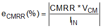
where
- VCM is the maximum operational AC or DC voltage on the input of the device.